Three-dimensional shape measurement method of coated devices based on white light scanning interference

A technology of white light scanning and measurement method, applied in the field of measurement, can solve the problems of difficult measurement accuracy, limited measurement lateral resolution, and inapplicability of too thick film layers, etc., and achieves the effects of strong anti-noise performance, high calculation accuracy and convenient implementation.

Active Publication Date: 2019-04-30
SOUTH CHINA NORMAL UNIVERSITY
View PDF7 Cites 0 Cited by
  • Summary
  • Abstract
  • Description
  • Claims
  • Application Information

AI Technical Summary

Problems solved by technology

Compared with the photometric method, the ellipsometry has the advantage of high sensitivity, but the test results are greatly affected by the outside world, and a complex mathematical model is required to solve the thickness
Moreover, the ellipsometry has limitations in measuring film thickness, because it has periodic problems, and is not suitable for the measurement of too thick film layers. When the actual film thickness exceeds 1 μm, it is already difficult to measure accurately.
[0007] It can be seen that both photometry and ellipsometry have certain limitations. These two methods can only perform single-point measurement. If you want to obtain film thickness information within a certain range, you must perform horizontal two-dimensional scanning. The spot has a certain size, which limits the lateral resolution of the measurement
[0008] In summary, the above two methods can only measure the thickness of the film, but cannot measure the morphology of the substrate.
In practical applications, it is necessary to obtain film thickness information within a certain range and measure the three-dimensional shape of the substrate, which cannot be solved by traditional measurement methods.

Method used


Image

  • Three-dimensional shape measurement method of coated devices based on white light scanning interference
  • Three-dimensional shape measurement method of coated devices based on white light scanning interference
  • Three-dimensional shape measurement method of coated devices based on white light scanning interference

Examples


no. 1 example

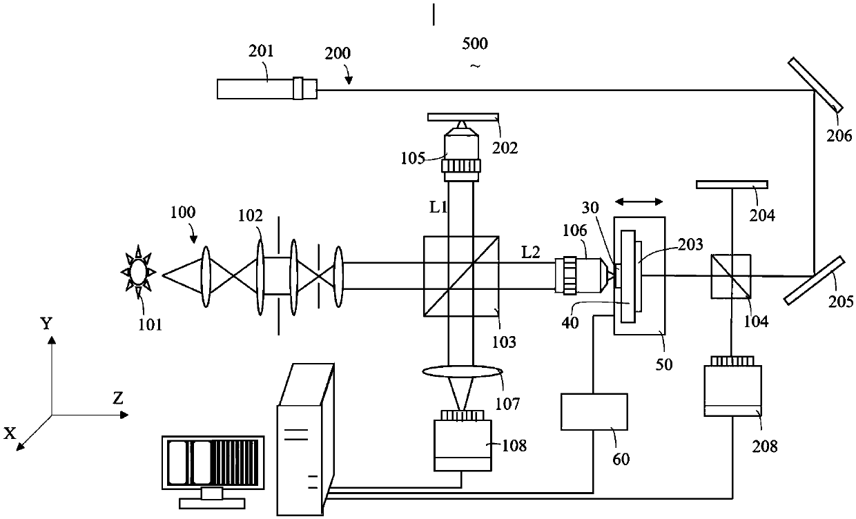
[0018] In this embodiment, a white light scanning interferometry system 500 will be described with reference to the accompanying drawings, which will be used as a hardware part for implementing the method for measuring the three-dimensional shape of a coated device in the second embodiment.

[0019] like figure 1 As shown, the white light scanning interferometry system 500 provided by the first embodiment of the present invention includes a white light scanning module 100, a calibration module 200, a fixed plate 40 for fixing the object to be measured 30, a piezoelectric ceramic micro-displacement platform 50, and a piezoelectric ceramic micro-displacement platform 50. Electroceramic controller 60.

[0020] Wherein the white light scanning module 100 comprises: a white light source 101, a Kohler illumination system 102, a first beam splitter 103 and a first plane mirror 202, a first microscope objective 105 and a second microscope objective 106 , an imaging lens 107 , and a f...

no. 2 example

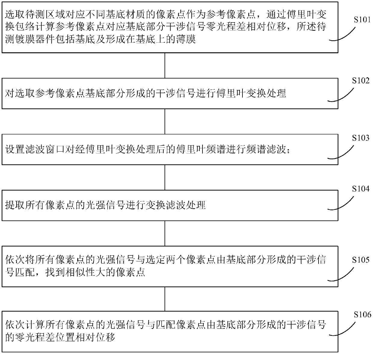
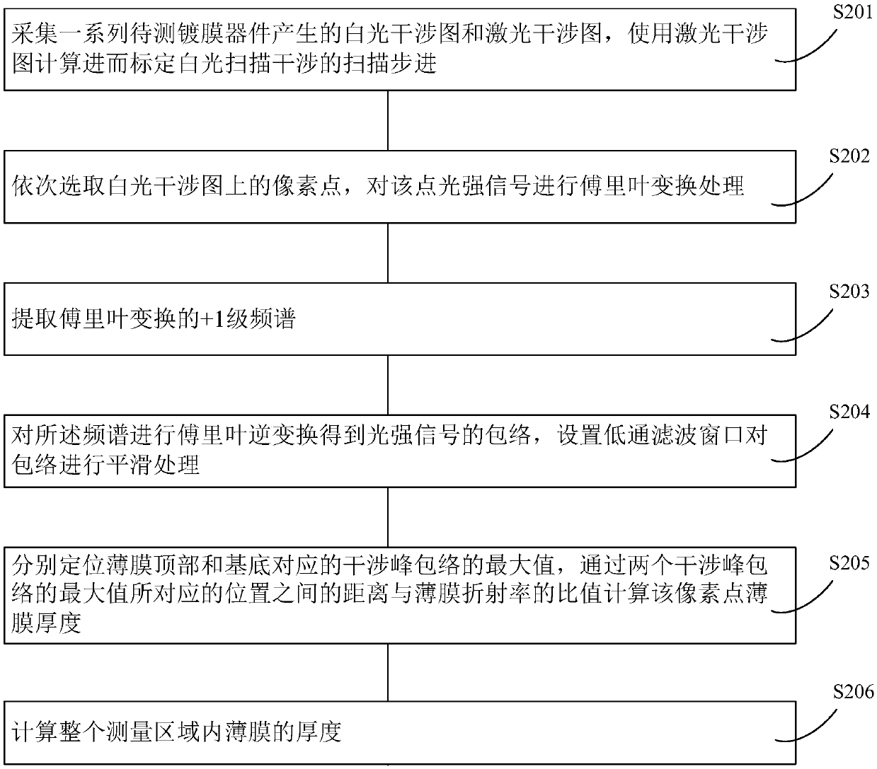
[0038] Please refer to figure 2 , the method for measuring the three-dimensional shape of a coated device based on white light scanning interference will be further described below in conjunction with the accompanying drawings and embodiments. In this method, the white light scanning interferometry system 500 described in the first embodiment is used for measurement, and specifically includes the following steps S201–S206.

[0039] In this embodiment, white light scanning interference is used to measure the topography of the coated device. In the case of different substrate materials of the coated device, the envelope shape of the first interference peak formed by the upper layer of the film is the same, while the second interference peak formed by the substrate The envelope shape of each interference peak will be different. In this embodiment, it is assumed that the substrate is composed of two materials.

[0040] Step S101, select pixels corresponding to different substra...


PUM


Abstract

The invention relates to a coated device three-dimensional topography measurement method based on white-light scanning interference. According to the method, a corresponding substrate part interference signal zero-optical-path-difference position extraction process is converted to a problem of calculating relative displacement of an interference signal between different pixels through a generalized related time delay estimation method, thereby accurately calculating substrate part three-dimensional topography information. Furthermore, the surface film thickness of a to-be-measured coated device can be obtained by means of the measurement method. The coated device three-dimensional topography measurement method has advantages of high calculation precision and high noise resistance. Central wavelength calibration of a light source is not required. Furthermore no requirement for envelope shape of a white-light interference signal is realized. High convenience is application is obtained.

Description

technical field [0001] The invention relates to the field of measurement, in particular to a method for measuring the three-dimensional shape of a coating device based on white light scanning interference. Background technique [0002] At present, the development of process technology has promoted the development of thin film technology, and the theory, process and measurement of thin film technology have formed a complete system. With the rapid development of micro-electro-mechanical system (Micro-Electro-Mechanical System, MEMS) devices and semiconductor devices, surface coating technology has been more applied. [0003] Due to the increasing importance of optical thin films, various technologies for detecting thin films have also developed rapidly. The measurement of thin films includes optical, mechanical, and electrical performance measurements. The measurement of optical properties includes macroscopic measurement of thin film, thin film thickness measurement and refr...

Claims


Application Information

Patent Timeline
Patent Type & Authority Patents(China)
IPC IPC(8): G01B11/24
CPCG01B11/2441
Inventor 吕晓旭蔡红志周云飞刘胜德钟丽云
Owner SOUTH CHINA NORMAL UNIVERSITY
Why Eureka
Try Eureka