A microbolometer with high filling factor and its preparation method

A microbolometer and fill factor technology, applied in the direction of electric radiation detectors, can solve the problems of increased process difficulty, uneven deposition, excessive diameter, etc., to increase the difficulty of process, simple manufacturing process, occupy small area effect

Active Publication Date: 2018-12-07
YANTAI RAYTRON TECH
View PDF6 Cites 0 Cited by
  • Summary
  • Abstract
  • Description
  • Claims
  • Application Information

AI Technical Summary

Problems solved by technology

This method leads to a small proportion of pixels occupied by the thermistor, which affects the performance of the detector
Depositing the metal electrode film directly in the contact hole will lead to uneven deposition, which may cause the metal film not to be deposited on the bottom of the contact hole, and not be able to connect with the metal electrode of the readout circuit at the bottom, resulting in poor electrical connectivity. Affect the performance of the detector
The Tsinghua University patent (CN102798471A) bonds two silicon wafers with a detector structure and a CMOS circuit to realize the detector manufacturing, which increases the difficulty of the process; and the diameter of the through-silicon hole prepared by this structure is too large, even reaching 20μm, which brings great difficulties to the production of high-performance small-pixel microbolometers

Method used


Image

  • A microbolometer with high filling factor and its preparation method
  • A microbolometer with high filling factor and its preparation method
  • A microbolometer with high filling factor and its preparation method

Examples


Embodiment Construction

[0036] In order to further understand a microbolometer with a high filling factor of the present invention and its preparation method, the following examples are listed and described in detail with accompanying drawings. It should be understood that the embodiments shown in the drawings are not intended to limit the scope of the present invention, but to illustrate the essence of the technical solution of the present invention.

[0037] Its specific process steps:

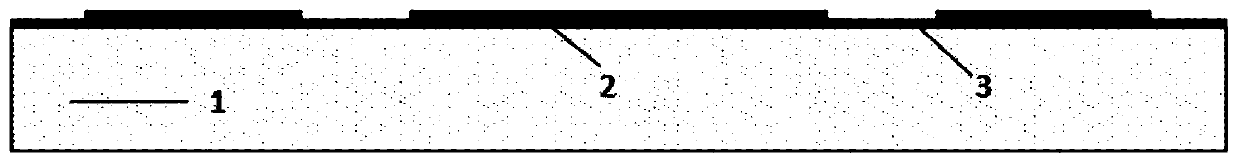
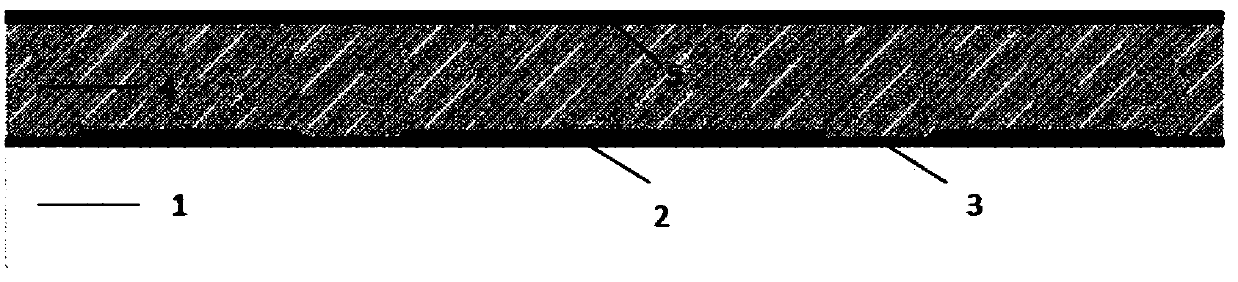
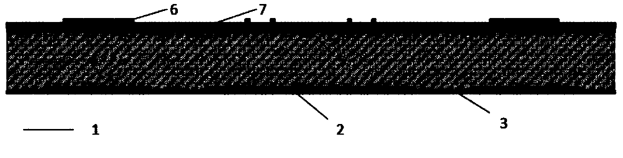
[0038]The metal reflective layer 2 is fabricated on the wafer with the processed readout circuit 1 as the base, the thickness of the film is 0.05-0.40 μm, and the metal reflective layer can be selected from Au, Cu, and Al. After etching the metal reflective layer 2, deposit a layer of silicon nitride film with a thickness of 0.02-0.30 μm on the reflective layer pattern as the insulating dielectric layer 3, such as figure 1 shown.

[0039] Preparation of the sacrificial layer 4, the sacrificial layer 4 can be mad...


PUM

PropertyMeasurementUnit
thicknessaaaaaaaaaa
thicknessaaaaaaaaaa
thicknessaaaaaaaaaa

Abstract

The invention relates to a microbolometer with a high filling factor and a preparation method thereof. A metal reflective layer (2), an insulating medium layer (3) and a sacrificial layer ( 4), after the support layer (5), metal electrode layer (6), thermal sensitive layer (8), and passivation layer (9), combine chemical mechanical polishing, tungsten plunger or physical vapor deposition, chemical vapor deposition, electrochemical Deposition and other technologies prepare electrical connection structures with high aspect ratios, reduce the area of ​​electrical connection structures, and increase the fill factor of microbolometers. Infrared or terahertz detectors based on microbolometers are composed of array microbolometers with large arrays. By reducing the area of ​​contact holes, the fill factor can be effectively improved, and the performance of the detector can be improved at the same time. . Using this structure, it is possible to design and manufacture microbolometers with smaller pixels in the future to reduce the pixel size proportionally without increasing the difficulty of the process.

Description

technical field [0001] The invention belongs to the field of microelectromechanical system (MEMS) process manufacturing in semiconductor technology, and in particular relates to a microbolometer with high filling factor and a preparation method. Background technique [0002] Micro-bolometer is a kind of heat detector based on the resistance value of the material with heat-sensitive characteristics changes correspondingly when the temperature changes. [0003] Uncooled infrared detection technology is a technology that senses the infrared radiation (IR) of external objects without a cooling system and converts it into an electrical signal that is processed and output on the display terminal. It can be widely used in many fields such as national defense, aerospace, medicine, production monitoring, etc. . Uncooled infrared focal plane detectors are able to work at room temperature, and have the advantages of light weight, small size, long life, low cost, low power, fast startu...

Claims


Application Information

Patent Timeline
Patent Type & Authority Patents(China)
IPC IPC(8): G01J5/20
CPCG01J5/20
Inventor 邱栋王鹏王宏臣陈文礼马宏
Owner YANTAI RAYTRON TECH
Why Eureka
Try Eureka