Capacitive structure and its preparation method, infrared detector with adjustable resonant band

A capacitive structure, infrared detection technology, applied in the field of infrared detectors, can solve the problems of low flexibility of use, application limitations of infrared detectors, etc., to achieve the effect of selectivity and avoidance of influence

Active Publication Date: 2018-10-16
SHANGHAI INTEGRATED CIRCUIT RES & DEV CENT
View PDF5 Cites 0 Cited by
  • Summary
  • Abstract
  • Description
  • Claims
  • Application Information

AI Technical Summary

Problems solved by technology

However, the selection of infrared absorbing materials with different absorption bands can only be one for an infrared detector. If the absorption band needs to be replaced, it is necessary to prepare infrared materials with other absorption bands, so that the application of infrared detectors is restricted. Restricted, and the flexibility of use is not high

Method used


Image

  • Capacitive structure and its preparation method, infrared detector with adjustable resonant band
  • Capacitive structure and its preparation method, infrared detector with adjustable resonant band
  • Capacitive structure and its preparation method, infrared detector with adjustable resonant band

Examples


Embodiment 1

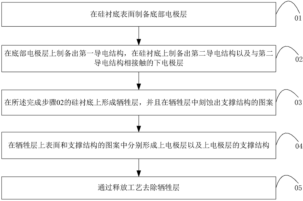
[0041] The following is attached Figure 1a~11 The present invention will be described in further detail with specific examples. It should be noted that the drawings are all in a very simplified form, using imprecise scales, and are only used to facilitate and clearly achieve the purpose of assisting in describing the present embodiment.

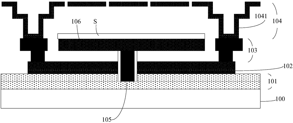
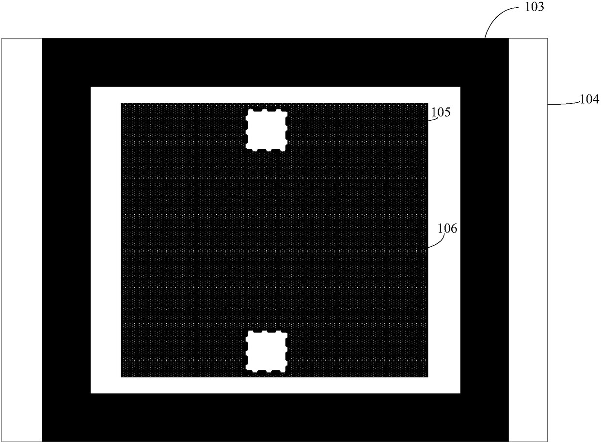
[0042] see Figure 1a , the surface of the silicon substrate 100 of this embodiment has an interconnection layer 101, and the capacitor structure integrated on the silicon substrate 100 includes:

[0043] The bottom electrode layer 102 is connected to the interconnection layer 101 on the silicon substrate 100, and serves as an extraction electrode of the upper electrode layer 104, and has a first conductive structure 103 on the edge region of the bottom electrode layer 102; the first conductive structure can be formed by the top Consists of conductive block and bottom conductive column;

[0044] The lower electrode layer 106 is located abo...

Embodiment 2

[0064] see Figures 12a to 12c ,in, Figure 12c , in order to clearly express the relationship between each part, choose the path of BB' to cut Figure 12a The capacitor structure in . Here, the upper surface of the silicon substrate 200 has an interconnection layer 201, a bottom electrode layer 202 is disposed on the interconnection layer 201, a lower electrode layer 206 is disposed above the bottom electrode layer 202, and an upper electrode layer 204 is disposed above the lower electrode layer 206, There is a support structure 2041 in the upper electrode layer 204 , and the support structure 2041 is in contact with the first conductive structure 203 . The specific structure and relationship of the bottom electrode layer 202 , the lower electrode layer 206 and the upper electrode layer 204 are the same as those of the bottom electrode layer 102 , the lower electrode layer 106 and the upper electrode layer 104 in the first embodiment.

[0065] The difference between the ca...


PUM


Abstract

The invention provides a capacitor structure and a preparation method thereof and an infrared detector with an adjustable resonant band. The capacitor structure comprises a bottom electrode layer located on a silicon substrate, a first conductive structure arranged in an edge region of the bottom electrode layer, a lower electrode layer located above the bottom electrode layer, a second conductive structure in contact with the lower electrode layer, and an upper electrode layer located above the lower electrode layer, wherein the bottom electrode layer is taken as a lead-out electrode of the upper electrode layer; a space is formed between the lower electrode layer and the bottom electrode layer; the second conductive structure is taken as the lead-out electrode of the lower electrode layer; a support structure is arranged in the edge region of the upper electrode layer; a hollow cavity is formed between the upper electrode layer and the lower electrode layer; the support structure is in contact with the first conductive structure; and when voltage is applied to the upper electrode layer and the lower electrode layer, the upper electrode layer and the bottom electrode layer form a shielding structure of the lower electrode layer. The capacitor structure provided by the invention does not affect a peripheral circuit; the application range is expanded; and the selectivity of the infrared detector on different resonant bands is also achieved.

Description

technical field [0001] The invention relates to the technical field of semiconductors, in particular to a capacitor structure, a preparation method thereof, and an infrared detector with adjustable resonance band. Background technique [0002] The infrared detector is a device that converts the incident infrared radiation signal into an electrical signal output. It uses a thermal element to detect the existence or movement of an object. The detector collects the infrared radiation from the outside and then gathers it on the infrared sensor. The infrared sensor uses a thermal element , the thermal element will output a signal when it receives a change in the temperature of the infrared radiation, convert it into an electrical signal, and then analyze the waveform of the electrical signal. [0003] Traditional infrared detectors usually use infrared absorbing materials with different absorption bands to select the infrared band detected by the infrared detector. However, the ...

Claims


Application Information

Patent Timeline
Patent Type & Authority Patents(China)
IPC IPC(8): H01L23/64H01L31/09
Inventor 康晓旭周炜捷袁超
Owner SHANGHAI INTEGRATED CIRCUIT RES & DEV CENT
Why Eureka
Try Eureka