
Light receiving and transmitting integrated device

A technology of optical transceiver and optical emission components, applied in the field of optical communication, can solve problems such as large electrical crosstalk, complex manufacturing process, and increased cost of integrated optical transceiver devices

Inactive Publication Date: 2016-11-23
SUZHOU CREALIGHTS TECH
View PDF7 Cites 0 Cited by
  • Summary
  • Abstract
  • Description
  • Claims
  • Application Information

AI Technical Summary

Problems solved by technology

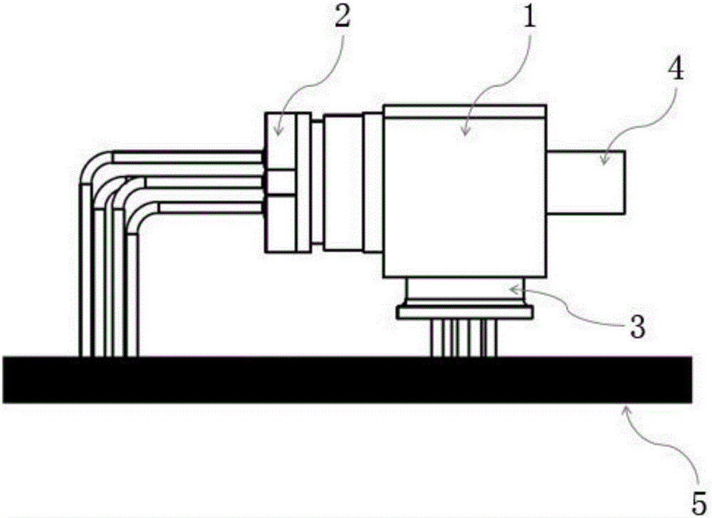
In order to form the above structure, the LD pin 2 needs to be bent by 90°, the manufacturing process is relatively complicated, and the cost of the entire optical transceiver device is increased
The LD pin 2 of the existing optical transceiver device is relatively long. When the optical transceiver device works under high frequency conditions, the LD pin 2 will generate a large electrical crosstalk. Working under high frequency conditions, the transmission performance of the optical transceiver device will be seriously affected
[0004] To sum up, the commonly used integrated optical transceiver devices can no longer meet the current industry's demand for low-cost optical devices, and have large electrical crosstalk under high-frequency conditions, and poor transmission performance

Method used


Image

  • Light receiving and transmitting integrated device
  • Light receiving and transmitting integrated device
  • Light receiving and transmitting integrated device

Examples


Embodiment Construction

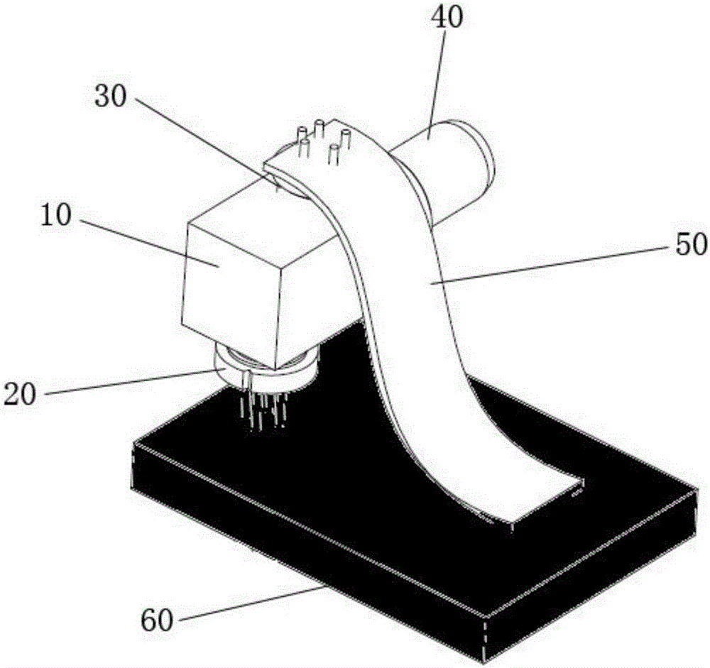
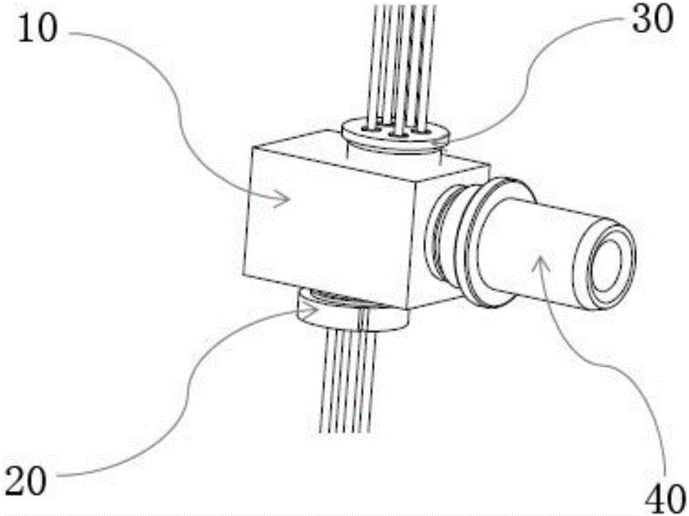
[0029] like figure 2 Shown is a schematic structural diagram of an integrated optical transceiver device of the present invention, the optical transceiver device is installed on a main board 60, and the main board 60 is connected to an optical fiber through the integrated optical transceiver device. The optical transceiver device includes a body 10 , an LD pin 20 , a PD pin 30 , an optical fiber connector 40 and a soft board 50 . The body 10 is connected to the motherboard 60 through the LD pin 20 . The PD pin 30 is located on the opposite side of the LD pin 20 and connected to the body 10 , and the PD pin 30 is connected to the main board 60 through the flexible board 50 . The fiber optic connector 40 is connected to the body 10 , and the body 10 is connected to an optical fiber through the fiber optic connector 40 . The main board 60 transmits electrical signals to the body 10 through the LD pins 20, and the body 10 performs electro-optical conversion through the optical ...


PUM


Abstract

The invention discloses an integrated optical transceiver device, which is installed on a main board, and the main board is connected to an optical fiber through the integrated optical transceiver device. The optical transceiver device includes a body, an LD pin, a PD pin, an optical fiber connector and a soft board. The body is connected to the motherboard through the LD pin. The PD pin is located on the opposite side of the LD pin and connected to the body, and at the same time, the PD pin is connected to the main board through the flexible board. The body is connected to an optical fiber through the optical fiber connector. The LD pin length of the optical transceiver integrated device is short, the electrical crosstalk is small in high frequency state, and the transmission performance is good.

Description

technical field [0001] The invention relates to the field of optical communication, in particular to an optical transceiver integrated device. Background technique [0002] Passive Optical Network (PON) is an optical access network that does not contain any electronic devices and electronic power supplies. Compared with active optical access networks, passive optical access networks are easy to maintain, High reliability and low cost. In recent years, with the continuous development of optical fiber communication, passive optical fiber access network has also been widely popularized by virtue of its excellent characteristics. In order to control the cost of passive optical fiber access network, manufacturers generally adopt BOSA on Board (BOB for short) technology at present, that is, install the Bi-direction Optical Sub-assembly (BOSA for short) directly on the mainboard, and reduce the Use item quantities to reduce product costs. [0003] like figure 1 Shown is a schem...

Claims


Application Information

Patent Timeline
IPC IPC(8): G02B6/42
CPCG02B6/4279G02B6/4296
Inventor 胡勇金梦溪胡朝阳
Owner SUZHOU CREALIGHTS TECH
Learn More