Routing layout method and wiring layout structure in bending area of flexible printed circuit board
A bending area, flexible printing technology, applied in the directions of printed circuits, printed circuit manufacturing, printed circuit components, etc., can solve the problem of affecting the use function and production yield, affecting the compactness of the LCM structure, and the overall circuit bending is not flat. and other problems, to achieve the effect of improving production efficiency, avoiding difficult bending and consistent softness
- Summary
- Abstract
- Description
- Claims
- Application Information
AI Technical Summary
Problems solved by technology
Method used
Image
Examples
Embodiment 1
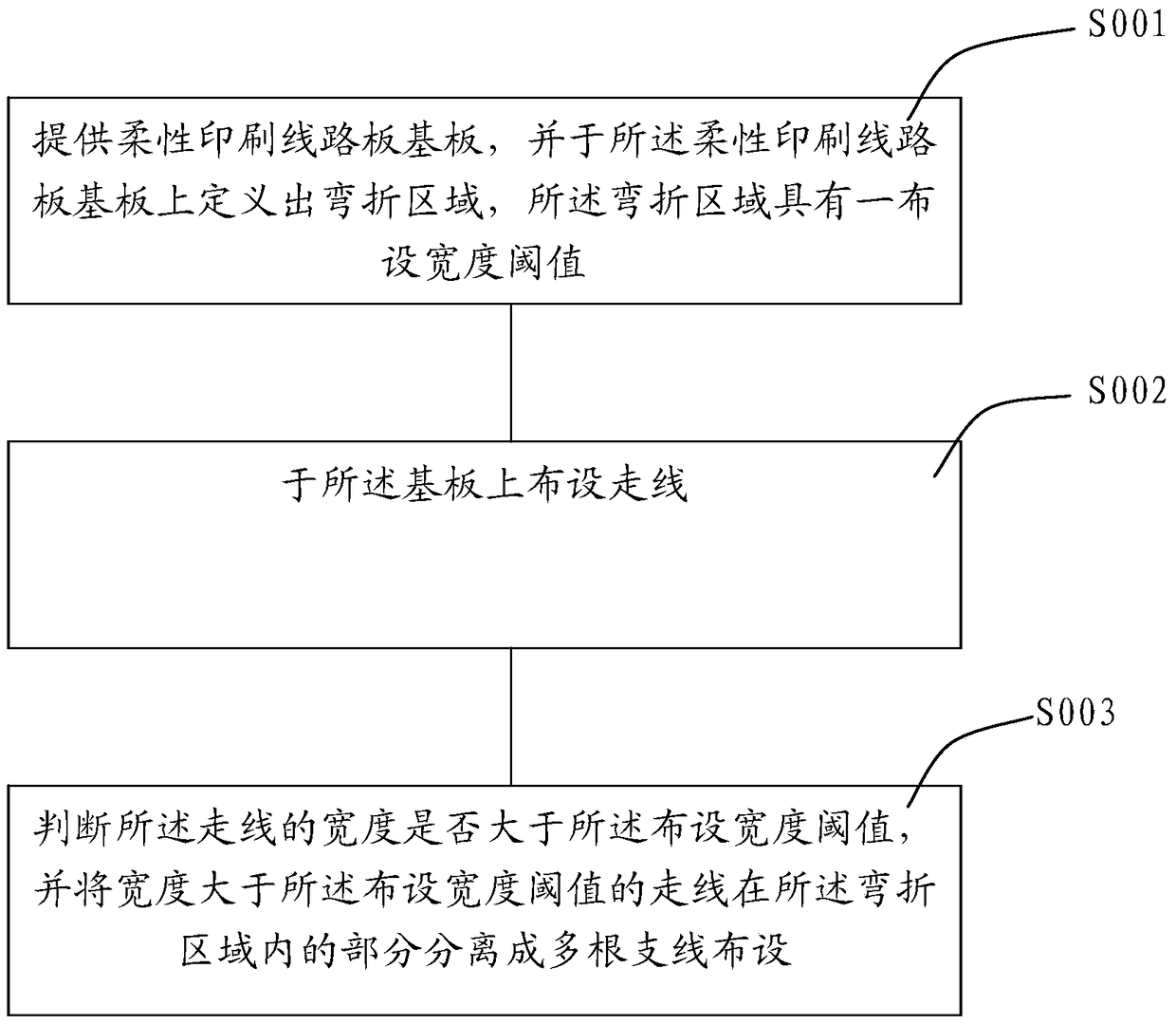
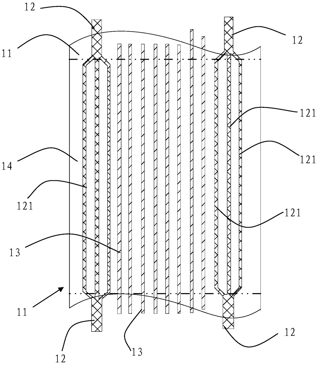
[0079] refer to image 3 As shown, firstly, a flexible printed circuit board substrate 11 is provided, and a bending area 14 is defined on the flexible printed circuit board substrate 11, and the bending area 14 has a layout for limiting the wiring in the bending area 14 a routing width threshold of width;
[0080] Next, lay out wiring on the flexible printed circuit board substrate 11, in this embodiment 1, the wiring includes power lines 12 and signal lines 13, wherein,
[0081] The width of the power line 12 is a;
[0082] The width of the signal line 13 is b;
[0083] Define the layout width threshold of the bending region 14 as c (c is the upper limit of the layout width threshold), where a>c>b;
[0084] Then, the part of the power line 12 outside the bending area 14 is laid on both sides of the flexible printed circuit board substrate 11 with a layout width of a;
[0085] When the power line 12 enters the bending area 14, it is judged whether the width a of the power...
Embodiment 2
[0089] still combined image 3 As shown, firstly, a flexible printed circuit board substrate 11 is provided, and a bending area 14 is defined on the flexible printed circuit board substrate 11, and the bending area 14 has a layout for limiting the wiring in the bending area 14 a routing width threshold of width;
[0090] Next, begin to lay out traces on the flexible printed circuit board substrate 11. In the second embodiment, the traces include power lines 12 and signal lines 13, wherein,
[0091] The width of the power line 12 is a;
[0092] The width of the signal line 13 is b;
[0093] Define the layout width threshold of the bending region 14 as c (c is the upper limit of the layout width threshold), where a>c, and b=c;
[0094] Then, the part of the power line 12 outside the bending area 14 is laid on both sides of the flexible printed circuit board substrate 11 with a layout width of a;
[0095] When the power line 12 enters the bending area 14, it is judged whether...
Embodiment 3
[0100] refer to Figure 4 As shown, firstly, a flexible printed circuit board substrate 11 is provided, and a bending area 14 is defined on the flexible printed circuit board substrate 11, and the bending area 14 has a layout for limiting the wiring in the bending area 14 a routing width threshold of width;
[0101] Next, begin to lay out traces on the flexible printed circuit board 11, in the third embodiment, the traces include power lines 12 and signal lines 13, wherein,
[0102] The width of the power line 12 is a;
[0103] The width of the signal line 13 is b;
[0104] Define the layout width threshold of the bending region 14 as c (c is the upper limit of the layout width threshold), where a>b>c;
[0105] Then, the part of the power line 12 outside the bending area 14 is laid out with a layout width of a;
[0106] When the power line 12 enters the bending area 14, it is determined whether the set width value a is greater than the layout width threshold c of the bendi...
PUM
 Abstract
Description
Claims
Application Information


