A silicon-based microdisplay

A technology of micro-display and display devices, which is applied to static indicators, instruments, etc., can solve the problems of reducing the amount of transmitted data and low utilization rate of screen display, and achieve the goal of improving pixel utilization rate, system performance and utilization rate Effect

Active Publication Date: 2019-01-11
LUMICORE MICROELECTRONICS SHANGHAI CO LTD
View PDF6 Cites 0 Cited by
  • Summary
  • Abstract
  • Description
  • Claims
  • Application Information

AI Technical Summary

Problems solved by technology

[0005] At present, the 4:3 or 16:9 rectangular display mainly used in VR display equipment has invalid display of the border display area, and the utilization rate of the screen display is not high, while the square display can effectively reduce the amount of transmitted data while improving the display capacity. of pixel utilization

Method used


Image

  • A silicon-based microdisplay
  • A silicon-based microdisplay
  • A silicon-based microdisplay

Examples


Embodiment 1

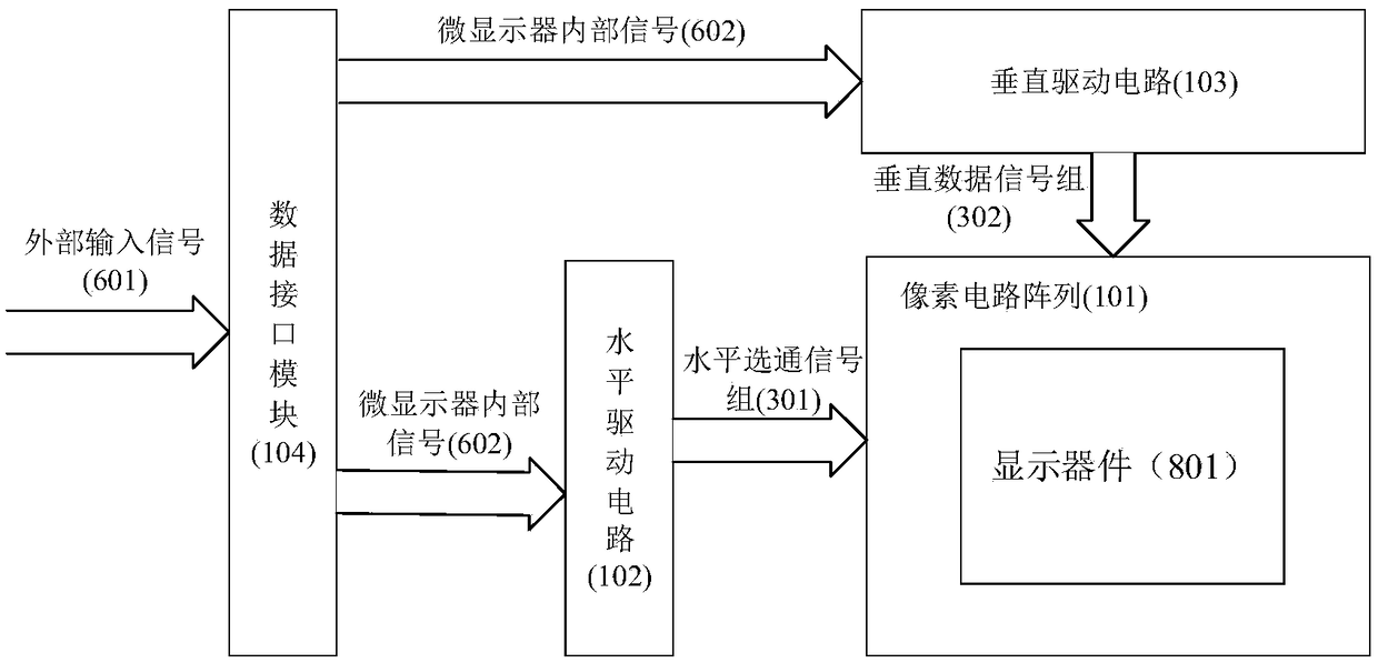
[0061] see figure 1 , a silicon-based microdisplay is characterized in that a silicon-based driving circuit (100) and a display device (801) are integrated on the same semiconductor silicon chip, the display device (801) is located on the surface of the semiconductor silicon chip, and the silicon The base drive circuit (100) includes:

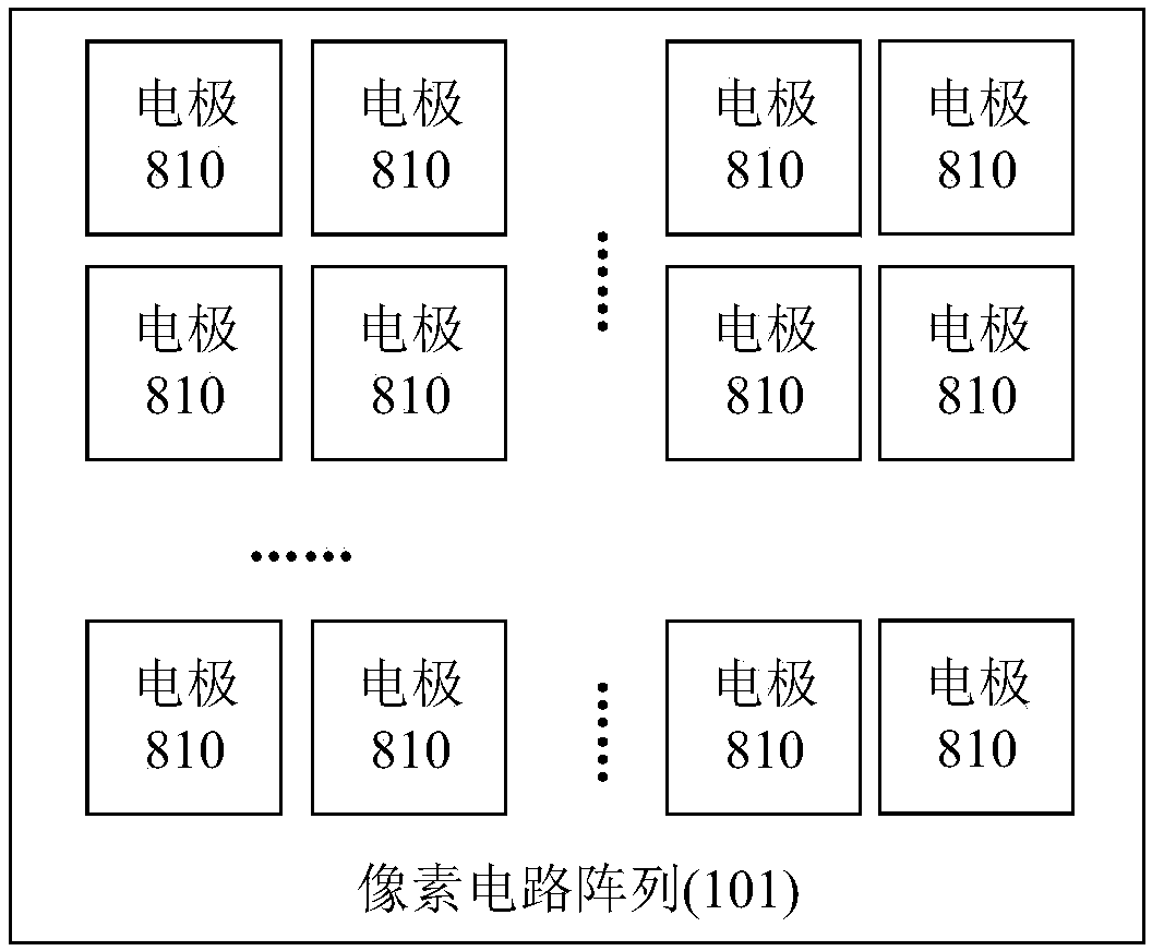
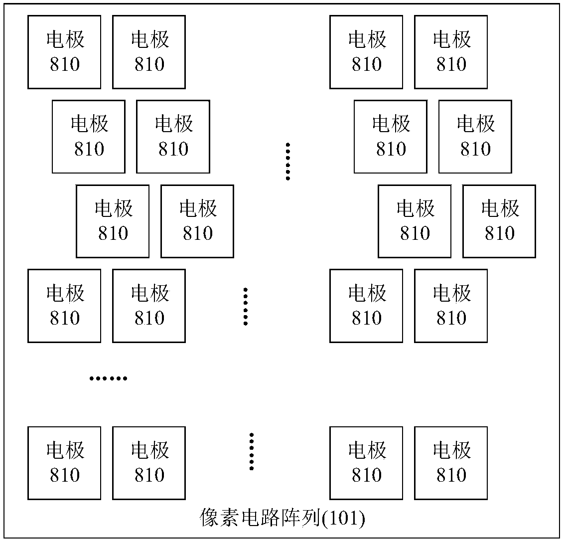
[0062] (1) Pixel circuit array (101), consisting of M×N pixel units, M, N are integers greater than or equal to 1 and M=N, the number of pixels in the horizontal direction and the vertical direction is equal, each pixel unit can Generate the voltage and current required by the display device (801), and drive the display device (801) to emit light;

[0063] (2) a horizontal drive circuit (102), used to generate a horizontal signal group (301) for horizontal display control of the pixel array (101);

[0064] (3) a vertical direction driving circuit (103), for generating a vertical data signal group (302) for use by pixels of the pixel circuit a...

Embodiment 2

[0074] This embodiment is basically the same as Embodiment 1, and the special features are as follows:

[0075] see Figure 11 A silicon-based microdisplay pixel circuit array drive circuit also includes an interface conversion module (105); the interface conversion module (105) converts the internal microdisplay (602) into a horizontal signal (400) and a vertical signal (500) ;

Embodiment 3

[0077] see Figure 12 , the pixel circuit unit in the pixel circuit array (101) is composed of a memory unit (111) and a drive unit (112); the memory unit (111) is used to save the switch state of the pixel, and its input is a horizontal selection Through signal (311) and vertical data signal (312); Described horizontal strobe signal (311) is a signal in the horizontal strobe signal group (301), is used for strobing this row to be effective; Described column data signal ( 312) is a signal in the vertical data signal group (302), used to represent the data signal of the column; the memory unit (111) and the drive unit (112) use the same positive power supply.

[0078] The memory unit (111) can be a static memory unit or a dynamic memory unit, the static memory unit does not have a capacitor, and is composed of 4-10 transistors, and the dynamic memory cell is composed of 1-2 capacitors and 1-3 Composed of transistors; the transistors are metal-oxide semiconductor field effect t...


PUM


Abstract

The invention relates to a silicon-based micro-displayer A drive circuit of the micro-displayer and a pixel unit are commonly integrated on a same one silicon-based chip to form a silicon-based micro-displayer. The drive circuit comprises four modules including a pixel circuit array, a row drive circuit, a column drive circuit and a data interface module; the characteristics of the silicon-based micro-displayer are that: the quantity of the pixel points in a horizontal direction in the pixel circuit array are the same as the quantity of the pixel points in a vertical direction to form a square displayer; the silicon-based displayer adopts the data interface to convert a data signal inputted from the outside to a micro-display internal signal, and transmission of display data is finished through the row drive circuit and the column drive circuit. The silicon-based micro-displayer can adopt a simulation driving method or a digital driving method to drive pixels to emit light.

Description

technical field [0001] The invention relates to the field of semiconductor displays, in particular to a silicon-based microdisplay. Background technique [0002] Silicon-based microdisplay is a combination of a display and a monocrystalline silicon integrated circuit. Its obvious feature is that the display is based on a monocrystalline silicon chip prepared with a CMOS drive circuit. Second, the size of the display is very small, and the image information needs to be enlarged by a certain optical system. . CMOS technology has the characteristics of low cost and small volume, and is the cornerstone of the integrated circuit industry. Silicon-based microdisplays have small pixel sizes that can produce higher display resolutions. [0003] The driving methods of silicon-based microdisplays are divided into analog driving and digital driving. The brightness of the OLED pixel in the analog driving circuit is proportional to the amplitude of the input current or voltage; while i...

Claims


Application Information

Patent Timeline
Patent Type & Authority Patents(China)
IPC IPC(8): G09G3/32G09G3/3208G09G3/20G09G3/3225G09G3/36
CPCG09G3/2096G09G3/32G09G3/3208G09G3/3225G09G3/3648G09G2330/02
Inventor 季渊王成冉峰
Owner LUMICORE MICROELECTRONICS SHANGHAI CO LTD
Why Eureka
Try Eureka