SRAM unit

A technology of transistors and transfer transistors, applied in information storage, static memory, digital memory information, etc., can solve the problems of large lead tasks, heavy loads, and reduced service life, and achieve the effect of high working stability

Inactive Publication Date: 2016-12-07
SEMICON MFG INT (SHANGHAI) CORP
View PDF4 Cites 0 Cited by
  • Summary
  • Abstract
  • Description
  • Claims
  • Application Information

AI Technical Summary

Problems solved by technology

In this way, the limited size of the second interconnection layer 17 requires three groups of control circuits to be connected. Compared with the first interconnection layer 16,

Method used


Image

  • SRAM unit
  • SRAM unit
  • SRAM unit

Examples


no. 2 example

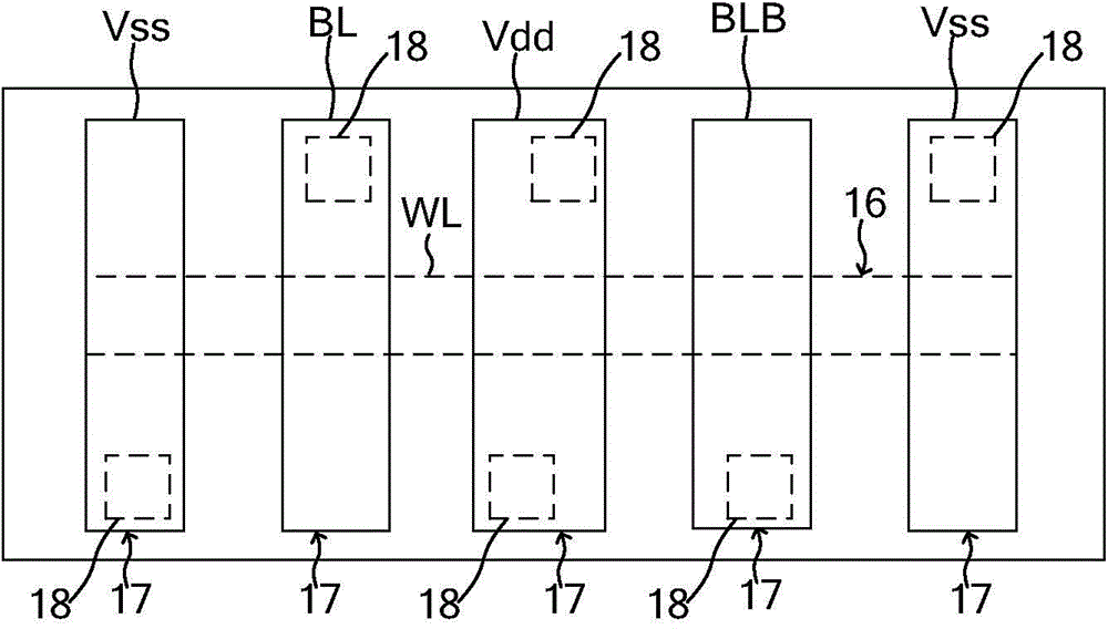
[0094] refer to Figure 5 , compared with the first embodiment, the difference of the second embodiment is:

[0095] The first interconnection layer 60' includes a word line WL and two power supply lines Vdd;

[0096] The second interconnection layer 70' includes a first bit line BL, a second bit line BLB, and two ground lines Vss.

[0097] Correspondingly, the first interconnection layer 60' further includes: a first interconnection 61 located below each grounding line Vss, and the grounding line Vss is electrically connected to the lower first interconnection 61 through a first-layer conductive plug 81'. connect.

[0098] In this embodiment, in the first interconnection layer 60', it is necessary to control the signals on the word line WL and the power connection Vdd through two different peripheral control circuits, and the first interconnection layer 60' needs to arrange two sets of peripheral Control circuit access. In contrast, in the second interconnection layer 70'...

no. 3 example

[0103] refer to Figure 6 , compared with the first and second embodiments, the difference of the third embodiment is:

[0104] The first interconnection layer 600 includes: a first bit line BL, a second bit line BLB and a power connection Vdd;

[0105] The second interconnection layer 700 above the first interconnection layer 600 includes: a word line WL and two ground lines Vss.

[0106] Compared with the first and second embodiments, in this embodiment, the first bit line BL and the second bit line BLB are located between the zero-level interconnection layer (not shown in the figure) and the second interconnection layer 700 between. The word line WL is a stronger signal line than the first and second bit lines, and the first bit line BL and the second bit line BLB are weaker signal lines. The interconnection layer of the peripheral control circuit of the SRAM unit is erected above the SRAM unit. When the first and second bit lines are above the word line WL, the signals ...

no. 4 example

[0109] refer to Figure 7 , compared with the third embodiment, the difference of the fourth embodiment is:

[0110] The first interconnect layer 620 includes: a first bit line BL, a second bit line BLB and a ground line Vss;

[0111] The second interconnection layer 720 includes: a word line WL and two power lines Vdd. Compared with the third embodiment, the two power supply lines Vdd of the present embodiment are separated into two parts by the word line WL.


PUM


Abstract

The invention discloses an SRAM (Static Random Access Memory) unit. A first transmission transistor comprises a first source and a first gate; a first pull-down transistor comprises a second source; a second transmission transistor comprises a third source and a second gate; a second pull-down transistor comprises a fourth source electrode; a first pull-up transistor comprises a fifth source; a second pull-up transistor comprises a sixth source; in first and second interconnection line layers, one interconnection line layer comprises a word line and a power supply connection line, the other interconnection line layer comprises first and second bit lines and a grounding line, or one interconnection line layer comprises the word line and the grounding line, and the other interconnection line layer comprises the first and second bit lines and the power supply connection line; the word line is electrically connected with the first and second gates; the first bit line is electrically connected with the first source; the second bit line is electrically connected with the third source; the power supply connection line is electrically connected with the fifth and sixth sources; and the grounding line is electrically connected with the second and fourth sources. According to the scheme, the number of peripheral control circuits arranged on the first interconnection line layer is the same as the number of peripheral control circuits arranged on the second interconnection line layer; and supported lead tasks are basically balanced.

Description

technical field [0001] The invention relates to the technical field of semiconductors, in particular to an SRAM unit. Background technique [0002] Static Random Access Memory (SRAM), as a member of memory, has the advantages of high speed, low power consumption and compatibility with standard processes, and is widely used in PCs, personal communications, consumer electronics (smart cards, digital cameras, Multimedia player) and other fields. [0003] A static random access memory includes a plurality of static random access memory units (hereinafter referred to as SRAM units), and the plurality of SRAM units are arranged in an array. refer to figure 1 , figure 1 It is a schematic diagram of the layout structure of an SRAM cell comprising six transistors (6-T) in the prior art, and the SRAM cell includes: [0004] The first pass NMOS transistor PG1 and the first pull-down NMOS transistor PD1, PG1 has a first source 1 and a first gate 2, PD1 has a second source 3, PG1 and...

Claims


Application Information

Patent Timeline
IPC IPC(8): G11C11/413
Inventor 张弓
Owner SEMICON MFG INT (SHANGHAI) CORP
Why Eureka
Try Eureka