NAND flash memory array architecture having low read latency and low program disturb
A NAND flash and memory technology, applied in the field of NAND flash memory array architecture, can solve the problems of long read delay time and limitation, achieve low power consumption, reduce read delay, and high memory density Effect
- Summary
- Abstract
- Description
- Claims
- Application Information
AI Technical Summary
Problems solved by technology
Method used
Image
Examples
Embodiment Construction
[0051] The illustrated embodiments or examples of the invention will be described as follows. The scope of the present invention is not limited thereto. Those skilled in the art should be able to understand that some modifications, substitutions and substitutions can be made without departing from the spirit and structure of the present invention. In the embodiments of the present invention, element symbols may be used repeatedly, and several embodiments of the present invention may share the same element symbols, but the characteristic elements used in one embodiment are not necessarily used in another embodiment.
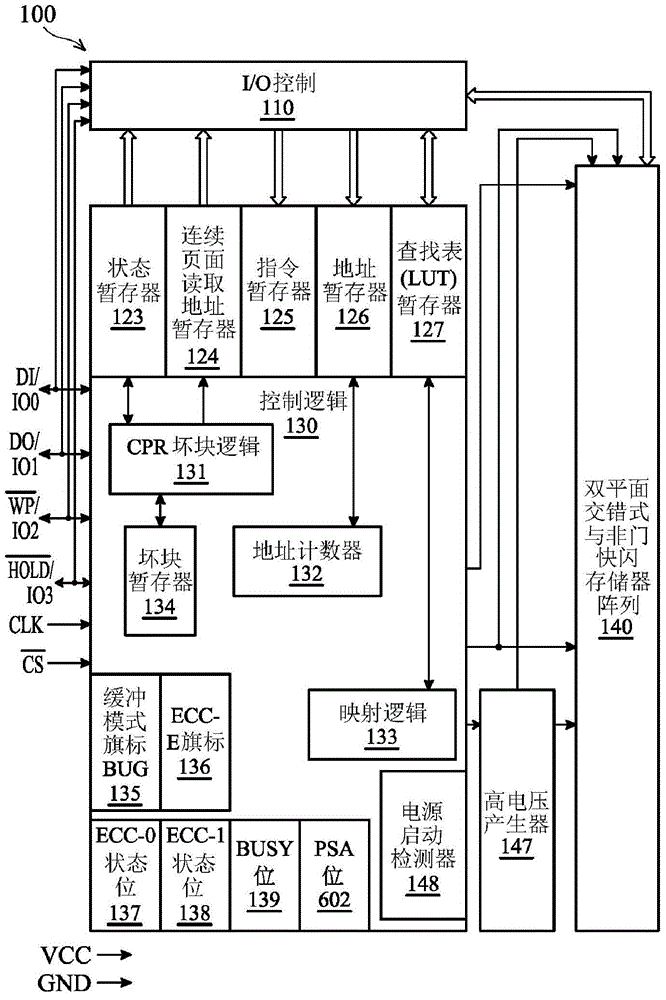
[0052] In order to compete with NOR flash memory devices in specific applications, NAND flash memory devices should have the following characteristics, including: (1) Multiple input / output serial peripheral interface (SPI) or multiple input / output quad Peripheral interface (Quad Peripheral Interface, QPI); (2) Small size and low pin count package type (density as...
PUM
 Abstract
Description
Claims
Application Information


