Supercharge Your Innovation With Domain-Expert AI Agents!

Chip package side wall ball planting process

Active Publication Date: 2019-01-04
NAT CENT FOR ADVANCED PACKAGING CO LTD
View PDF4 Cites 2 Cited by
  • Summary
  • Abstract
  • Description
  • Claims
  • Application Information

AI Technical Summary

Problems solved by technology

[0005] In view of the above-mentioned and / or the problem that two-dimensional packaged chips cannot be wired or welded on the sidewalls existing in existing semiconductor packages, the present invention is proposed

Method used


Image

  • Chip package side wall ball planting process
  • Chip package side wall ball planting process
  • Chip package side wall ball planting process

Examples


Embodiment Construction

[0039] In order to make the above objects, features and advantages of the present invention more comprehensible, the specific implementation manners of the present invention will be further described below in conjunction with specific drawings.

[0040] In the following description, a lot of specific details are set forth in order to fully understand the present invention, but the present invention can also be implemented in other ways that are different from those described here, and those skilled in the art can do so without departing from the connotation of the present invention. By analogy, the present invention is not limited by the specific examples disclosed below.

[0041] Secondly, the present invention is described in detail in combination with schematic diagrams. When describing the embodiments of the present invention in detail, for the convenience of explanation, the cross-sectional view showing the device structure will not be partially enlarged according to the g...


PUM


Abstract

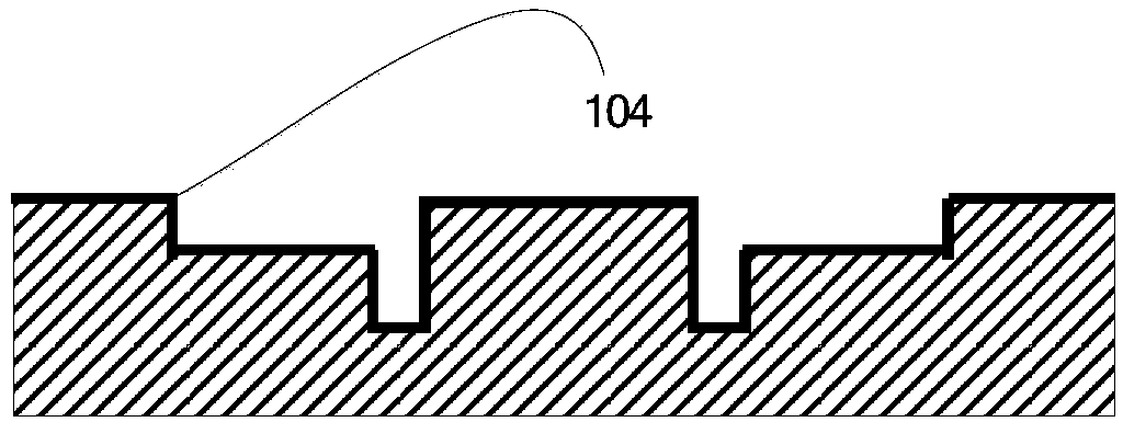
The invention relates to a chip packaging side wall bumping process. The chip packaging side wall bumping process is characterized by including the following steps that 1, an RDL wire routing layer and TSV holes are made on a wafer, TSV hole metals are made in the TSV holes, and the connecting positions between the tail end of the RDL wire routing layer and the TSV holes serve as bonding pads; 2, grooves are formed in the wafer to expose the side faces or the side faces and the bottom surfaces of the TSV hole metals; 3, the bumping process is conducted on the upper surface of the tail end of the RDL wire routing layer, and convex points are formed on the side walls of the bonding pads and the side walls of the TSV hole metals after reflux; 4, chip separation is performed through cutting or back thinning to obtain a single chip with convex points on the side walls. The chip packaging side wall bumping process makes the metal bonding pads exposed through an etching process, avoids pollution of metal ions to a silicon material and performs bumping on the surface of the wafer, and solder balls exist on the peripheral side wall of the wafer and facilitate side wall welding.

Description

technical field [0001] The invention relates to a chip packaging side wall ball planting process, which belongs to the technical field of semiconductors. Background technique [0002] With the development of semiconductor technology, the feature size of integrated circuits continues to shrink, and the interconnection density of devices continues to increase. The traditional two-dimensional packaging can no longer meet the needs of the industry. The key technical advantages of interconnection, high-density integration and low cost have gradually led the development trend of packaging technology. However, in general two-dimensional packaging, there are no pads or bumps around the side walls of the chip, and the wiring can only be the front PAD (pad) of the chip corresponding to the front PAD or gold finger of the connection end, so these chips cannot be used for side wall bonding. Wire or solder. [0003] In the process of front-side assembly of the adapter board chip, it is...

Claims


Application Information

Patent Timeline
Patent Type & Authority Patents(China)
IPC IPC(8): H01L21/768H01L21/60
CPCH01L21/76805H01L24/03H01L24/11H01L2224/0231H01L2224/1146H01L2224/11
Inventor 薛海韵冯光建
Owner NAT CENT FOR ADVANCED PACKAGING CO LTD
Features
  • R&D
  • Intellectual Property
  • Life Sciences
  • Materials
  • Tech Scout
  • Unparalleled Data Quality
  • Higher Quality Content
  • 60% Fewer Hallucinations
Learn More