A flip-chip led microdisplay array and manufacturing method thereof

A flip-chip, micro-display technology, applied in semiconductor/solid-state device manufacturing, semiconductor devices, electrical components, etc., can solve the problems of inter-pixel light interference, spot enlargement, etc., to achieve the effect of improving resolution and reducing interference

Active Publication Date: 2019-09-03
上海君万微电子科技有限公司
View PDF5 Cites 0 Cited by
  • Summary
  • Abstract
  • Description
  • Claims
  • Application Information

AI Technical Summary

Problems solved by technology

However, light from the light-emitting layer of such a high-density LED pixel array is emitted through n-GaN and sapphire substrates, and it is easy to cause light interference between pixels and enlargement of light spots.

Method used


Image

  • A flip-chip led microdisplay array and manufacturing method thereof
  • A flip-chip led microdisplay array and manufacturing method thereof
  • A flip-chip led microdisplay array and manufacturing method thereof

Examples


Embodiment Construction

[0032] The technical solutions of the present invention will be described in detail below in conjunction with specific embodiments.

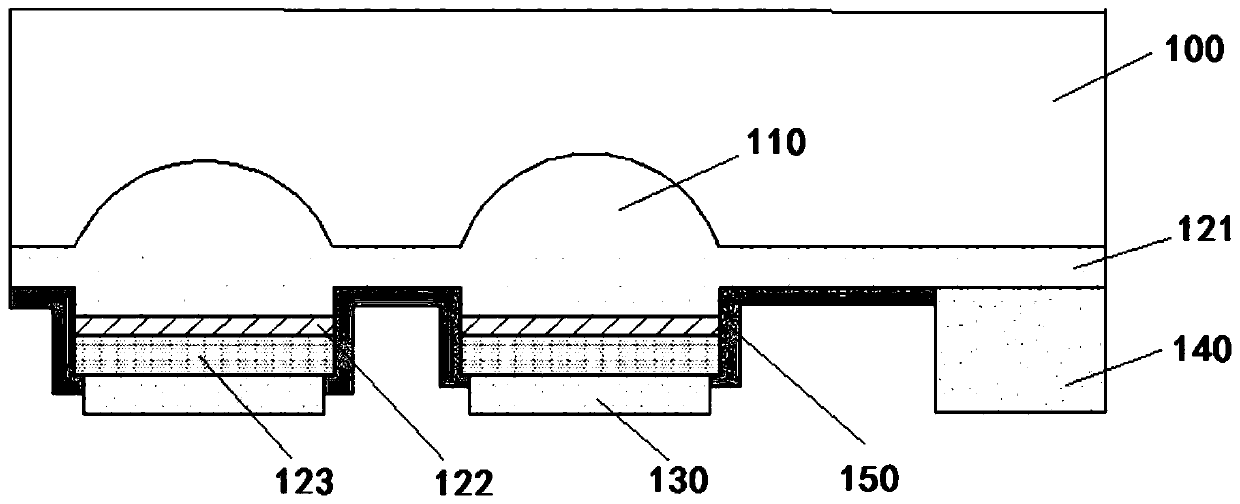
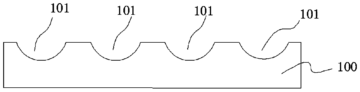
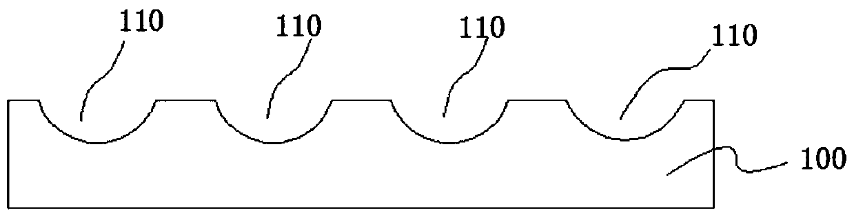
[0033] Such as figure 1 A LED micro-display array flip-chip shown includes a sapphire substrate 100, a plurality of grooves 101 etched in an array on the sapphire substrate 100, a transparent film layer 110 filled in the grooves 101 and deposited on the sapphire substrate. LED micro-pixel array on the bottom 100.

[0034] Such as figure 2 As shown, the grooves 101 are hemispherical grooves with a diameter of 5-25 μm, and the arrays are distributed on the substrate 100 at equal intervals. The transparent thin film layer 110 is filled in the groove 101, the transparent thin film layer 110 has a refractive index>2.3, and a transmittance of blue light or green light>97%.

[0035] Such as figure 1 with 5 As shown, each LED micro-pixel corresponds to the groove 101 one by one, and a SiOx or SiNx insulating layer 150 is provided between them. Th...


PUM


Abstract

The invention discloses an LED micro display array flip chip and a manufacturing method. The flip chip comprises a substrate, a plurality of grooves, a transparent thin film layer and an LED micro pixel array arranged on the substrate, wherein the plurality of grooves are etched in the substrate in an array; the grooves are filled with the transparent thin film layer; various LED micro pixels correspond to the grooves one by one; a refractive index of the transparent thin film layer is greater than 2.3; the transmittance on blue light or green light is greater than 97%; each LED micro pixel comprises an N-type GaN layer, a multi-quantum well layer and a P-type GaN layer which are sequentially deposited on the substrate; the N-type GaN layers of the LED micro pixel array are connected into a whole to form a common cathode, and an N electrode metal contact layer is deposited on the common cathode; and a P electrode metal contact layer is deposited on the P-type GaN layers in an LED micro pixel region. According to the LED micro display array flip chip, a transparent thin film layer material with a high refractive index is deposited on the substrate, so that better convergence of light-emitting layer light sources is achieved; the problem that light is diffused after entering a sapphire substrate with a low refractive index is solved; interference of outlet light between pixel units is reduced; and the resolution of the LED micro display array is improved.

Description

technical field [0001] The invention relates to LED micro-displays, in particular to an LED micro-display array flip-chip and a manufacturing method thereof. Background technique [0002] Light-emitting diode (LED) is a solid-state semiconductor device with high efficiency, energy saving, environmental protection, and long life. It is currently widely used in traffic indication, indoor and outdoor full-color display, LCD TV backlight, lighting, etc. The LED array-based micro-display technology is a display technology that integrates a high-density micro-sized ultra-high-brightness two-dimensional array of light-emitting diodes on a chip and uses a silicon-based cmos circuit to drive it. Compared with The OLED and LCoS micro-display systems in the prior art have the advantages of high brightness and high contrast, firmness, fast response, and low cost. [0003] Ultra-high brightness GaN-LED microdisplay is an active luminous monochrome display device with compact structure, ...

Claims


Application Information

Patent Timeline
Patent Type & Authority Patents(China)
IPC IPC(8): H01L27/12H01L21/77
Inventor 石素君许键张雪峰
Owner 上海君万微电子科技有限公司
Why Eureka
Try Eureka