LED (Light-Emitting Diode) chip and production method thereof
What is Al technical title?
Al technical title is built by PatSnap Al team. It summarizes the technical point description of the patent document.
A technology of LED chips and electrodes, applied in electrical components, circuits, semiconductor devices, etc., can solve the problems of decreasing effective area of light output, uneven current distribution, affecting luminous efficiency, etc., to improve luminous performance, uniform current density distribution, increase Effect of Luminous Efficiency
Inactive Publication Date: 2016-12-07
FOCUS LIGHTINGS SCI & TECH
View PDF3 Cites 5 Cited by
Summary
Abstract
Description
Claims
Application Information
AI Technical Summary
This helps you quickly interpret patents by identifying the three key elements:
Problems solved by technology
Method used
Benefits of technology
Problems solved by technology
The two electrodes of the LED chip with a lateral structure are on the same side of the LED chip, the P electrode is in the p-type GaN region of the LED epitaxial layer, and the N electrode is distributed in the n-type GaN region exposed by etching. The distribution of P and N electrodes is not equidistant, resulting in uneven current distribution in the n-type GaN and p-type GaN layers, thus affecting the luminous efficiency
[0004] In addition, see figure 1 As shown, in the traditional horizontal structure LED chip, the N electrodes 81' and 82' are arranged in the n-type GaN area exposed by etching, because the epitaxial layer needs to etch a larger area (the entire n-type area), and because the P electrode 91' , 92' and N electrodes 81', 82' are all distributed on the light-emitting surface of the LED chip, so the effective area of light-emitting is reduced, so the light-emitting efficiency is low
Method used
Image
Click on the blue label to locate the original text in one second.
Reading with bidirectional positioning of images and text.
Examples
Embodiment Construction
[0029] In order to enable those skilled in the art to better understand the technical solutions in the present invention, the technical solutions in the embodiments of the present invention will be clearly and completely described below in conjunction with the drawings in the embodiments of the present invention. Obviously, the described The embodiments are only some of the embodiments of the present invention, not all of them. Based on the embodiments of the present invention, all other embodiments obtained by persons of ordinary skill in the art without making creative efforts shall fall within the protection scope of the present invention.
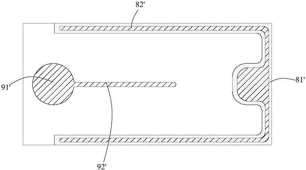
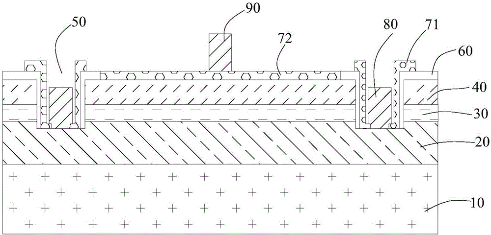
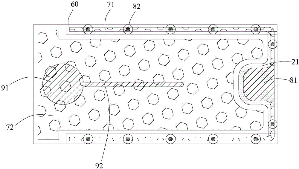
[0030] The invention discloses an LED chip, which comprises a substrate, an N-type semiconductor layer on the substrate, a light-emitting layer, a P-type semiconductor layer, and an N electrode electrically connected to the N-type semiconductor layer and the P-type semiconductor layer respectively. and P electrodes, the LED chip include...
PUM
Abstract
The invention provides an LED (Light-Emitting Diode) chip and a production method thereof. The LED chip comprises a substrate, an N-type semiconductor layer located on the substrate, a light-emitting layer, a P type semiconductor layer, and N electrodes and P electrodes which are electrically connected with the N-type semiconductor layer and the P type semiconductor layer. The LED chip also comprises an N type table surface and a plurality of N type electrode slots which are etched to the N-type semiconductor layer. Insulation dielectric layers crossing the N type electrode slots are arranged on the side walls of the N type electrode slots and above the P type semiconductor layer. First transparent conductive layers connected with the bottoms of the N type electrode slots and electrically connected with the N-type semiconductor layer are formed in the insulation dielectric layers. A first N electrode is arranged on the N type table surface. Second N electrodes are arranged in the first transparent conductive layers of the N type electrode slots. The first N electrode and the second N electrodes are electrically connected through the first transparent conductive layers. According to the LED chip provided by the invention, the current density distribution is even, the light-emitting performance of the LED chip is improved; the area of an active layer is increased effectively; and the light-emitting efficiency of the chip is improved.
Description
technical field [0001] The invention relates to the field of semiconductor chips, in particular to an LED chip and a manufacturing method thereof. Background technique [0002] A light-emitting diode (Light-Emitting Diode, LED) is a semiconductor electronic component that can emit light. This electronic component appeared as early as 1962. In the early days, it could only emit red light with low luminosity. Later, other monochromatic light versions were developed. Today, the light that can be emitted has covered visible light, infrared rays and ultraviolet rays, and the luminosity has also increased to a considerable extent. of luminosity. Because of its energy saving, environmental protection, safety, long life, low power consumption, low heat, high brightness, waterproof, miniature, shockproof, easy dimming, concentrated beam, easy maintenance, etc., it can be widely used in various indications, displays, decorations , backlight, general lighting and other fields. [00...
Claims
Application Information
Patent Timeline
Application Date:The date an application was filed.
Publication Date:The date a patent or application was officially published.
First Publication Date:The earliest publication date of a patent with the same application number.
Issue Date:Publication date of the patent grant document.
PCT Entry Date:The Entry date of PCT National Phase.
Estimated Expiry Date:The statutory expiry date of a patent right according to the Patent Law, and it is the longest term of protection that the patent right can achieve without the termination of the patent right due to other reasons(Term extension factor has been taken into account ).
Invalid Date:Actual expiry date is based on effective date or publication date of legal transaction data of invalid patent.