
Red LED epitaxial structure with high uniformity and preparation method of red LED epitaxial structure

An epitaxial structure and uniformity technology, which is applied in the direction of electrical components, circuits, semiconductor devices, etc., can solve the problems that the influence of the surface oxide layer cannot be eliminated, and the output rate of the die cannot be improved, so as to improve the uniformity of brightness and the finished product of the die Yield, Reduced Edge Effects, Effects of Reduced Deposition Effects

Active Publication Date: 2016-12-14
Shandong Huaguang Optoelectronics Co. Ltd.
View PDF6 Cites 11 Cited by
  • Summary
  • Abstract
  • Description
  • Claims
  • Application Information

AI Technical Summary

Problems solved by technology

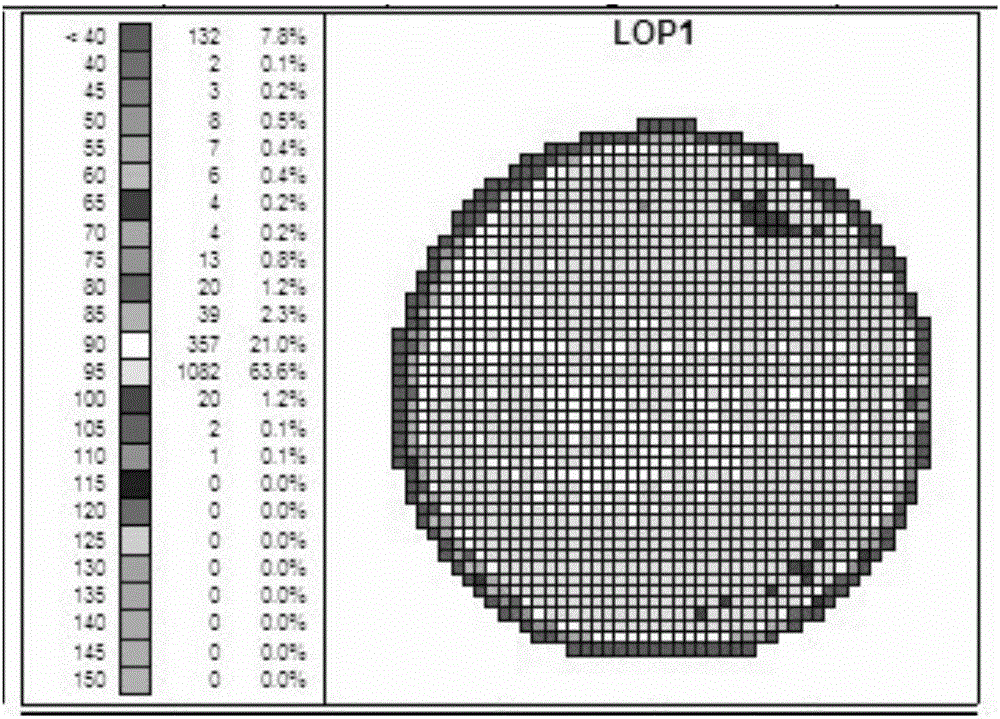
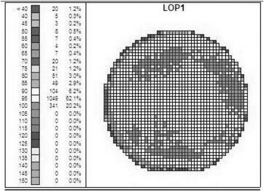
However, its disadvantage is that it cannot eliminate the influence of the surface oxide layer on the subsequent structure, and it cannot effectively improve the low-brightness part of the edge (less than 40mcd) to increase the output rate of the die.

Method used


Image

  • Red LED epitaxial structure with high uniformity and preparation method of red LED epitaxial structure
  • Red LED epitaxial structure with high uniformity and preparation method of red LED epitaxial structure
  • Red LED epitaxial structure with high uniformity and preparation method of red LED epitaxial structure

Examples


Embodiment 1

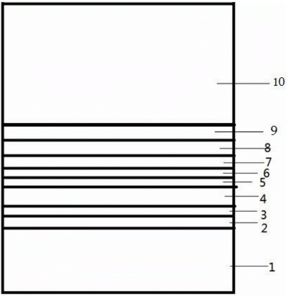
[0056] A high-uniformity red LED epitaxial structure, such as figure 1 As shown, it includes GaAs substrate 1, AlGaAs buffer layer 2, GaAs buffer layer 3, AlGaAs / AlAs DBR4, AlInP N confinement layer 5, AlGaInP N waveguide layer 6, MQW quantum well active layer 7 arranged in sequence from bottom to top , AlGaInP P waveguide layer 8, AlInP P confinement layer 9, GaP window layer 10.

[0057]The AlGaAs buffer layer 2 is used to eliminate the influence of the oxide layer on the surface of the GaAs substrate 1 on the epitaxial growth quality and improve the quality of the epitaxial growth; the GaAs buffer layer 3 is used to achieve perfect lattice matching with the GaAs substrate 1 to avoid the GaAs substrate 1 surface The defects and dislocations brought by the new growth material, and provide a fresh interface for the next growth; AlGaAs / AlAs DBR4 constitutes a composite Bragg reflection layer, which uses a periodic layered structure composed of two materials with different refra...

Embodiment 2

[0060] A kind of high uniformity red light LED epitaxial structure described in embodiment 1, its difference is that,

[0061] The thickness of the AlGaAs buffer layer 2 is 0.8 μm, and the carrier concentration is 5E18cm -3 . The thickness of GaAs substrate 1 is 375 μm; the thickness of GaAs buffer layer 3 is 0.5 μm, and the carrier concentration is 5E18cm -3 ; AlGaAs / AlAs DBR4 includes 30 pairs of AlGaAs / AlAs DBR4, the carrier concentration is 5E18cm -3 ; Each AlGaAs / AlAs DBR4 growth cycle period is a pair of AlGaAs / AlAs DBR4, and the AlGaAs / AlAs DBR4 logarithm can be grown according to the brightness required; the thickness of the AlInP N confinement layer 5 is 1 μm, and the carrier concentration is 5E18cm -3 , the III-V group ratio is 200; the AlGaInP N waveguide layer 6 has a thickness of 0.5 μm and is not doped, and the III-V group ratio is 350; the MQW quantum well active layer 7 has a thickness of 0.5 μm, is not doped, and has a III-V group ratio of 350. ratio is 350...

Embodiment 3

[0063] A kind of high uniformity red light LED epitaxial structure described in embodiment 1, its difference is that,

[0064] The thickness of the AlGaAs buffer layer 2 is 0.5 μm, and the carrier concentration is 6E17cm -3 . The thickness of GaAs substrate 1 is 310 μm; the thickness of GaAs buffer layer 3 is 0.4 μm, and the carrier concentration is 6E17cm -3 ; AlGaAs / AlAs DBR4 includes 15 pairs of AlGaAs / AlAs DBR4, the carrier concentration is 6E17cm -3 ; Each AlGaAs / AlAs DBR4 growth cycle period is a pair of AlGaAs / AlAs DBR4, and the AlGaAs / AlAs DBR4 logarithm can be adjusted according to the brightness required by the growth; the thickness of the AlInP N confinement layer 5 is 0.7 μm, and the carrier concentration is 6E17cm -3 , the III-V group ratio is 100; the AlGaInP N waveguide layer 6 has a thickness of 0.3 μm, no doping, and the III-V group ratio is 200; the MQW quantum well active layer 7 has a thickness of 0.3 μm, undoped, and the III-V group ratio is 0.3 μm. rat...


PUM


Abstract

The invention relates to a red LED epitaxial structure with high uniformity and a preparation method of the red LED epitaxial structure. The red LED epitaxial structure comprises a GaAs substrate, an AlGaAs buffer layer, a GaAs buffer layer, an AlGaAs / AlAs DBR, an AlInP N limiting layer, an AlGaInP N waveguide layer, an MQW quantum well active layer, an AlGaInP P waveguide layer, an AlInP P limiting layer and a GaP window layer. The AlGaAs buffer layer grows before growth of the GaAs buffer layer, and a surface oxidation layer is decomposed and absorbed through the AlGaAs buffer layer, so that the influence of the surface oxidation layer of the substrate on the subsequent epitaxial structure is reduced to the maximal extent.

Description

technical field [0001] The invention relates to a highly uniform red LED epitaxial structure and a preparation method thereof, belonging to the technical field of light emitting diodes. Background technique [0002] LED is the abbreviation of Light Emitting Diode (Light Emitting Diode). [0003] In the PN junction of some semiconductor materials, the energy released during the recombination of carriers will be emitted in the form of light, which directly converts electrical energy into light energy. Light-emitting recombination is formed by injecting carriers, and diodes made using this injection-type electroluminescent principle are light-emitting diodes, commonly known as LEDs. [0004] The luminous efficiency and luminous color of LED depend on the material and process of making LED. At present, the colors widely used are red, blue, green, white and yellow. Due to the low working voltage of LED (only 1.5 ~ 3V), its brightness can be adjusted by voltage (or current), and...

Claims


Application Information

Patent Timeline
Patent Type & Authority Applications(China)
IPC IPC(8): H01L33/12H01L33/30H01L33/00
CPCH01L33/0062H01L33/12H01L33/30
Inventor 张雨张新于军徐现刚
Owner Shandong Huaguang Optoelectronics Co. Ltd.
Learn More