Semiconductor module

A semiconductor and wiring layer technology, applied in the field of semiconductor modules, can solve problems such as inability to suppress surges, malfunctions, and insufficient low inductance

Active Publication Date: 2016-12-21
DENSO CORP
View PDF3 Cites 5 Cited by
  • Summary
  • Abstract
  • Description
  • Claims
  • Application Information

AI Technical Summary

Problems solved by technology

[0005] However, in the semiconductor module disclosed in Patent Document 1, even if the distance between the input and output terminals and the control board and the distance between the control terminals and the control board are minimized, it does not take into account the distance between the input and output terminals and the input Distance between output terminal and control terminal, etc.
For example, if the distance between the positive terminal and the negative terminal as the main terminal corresponding to the input terminal for current input among the input and output terminals is long, the inductance of the main circuit will increase.
In addition, if the distance between the main

Method used


Image

  • Semiconductor module
  • Semiconductor module
  • Semiconductor module

Examples


Example

[0067] (First embodiment)

[0068] The first embodiment of the present disclosure will be described. In this embodiment, as an application example of the semiconductor module of one embodiment of the present disclosure, for example, a semiconductor module included in a three-phase inverter circuit that drives a three-phase AC motor or the like is cited and described.
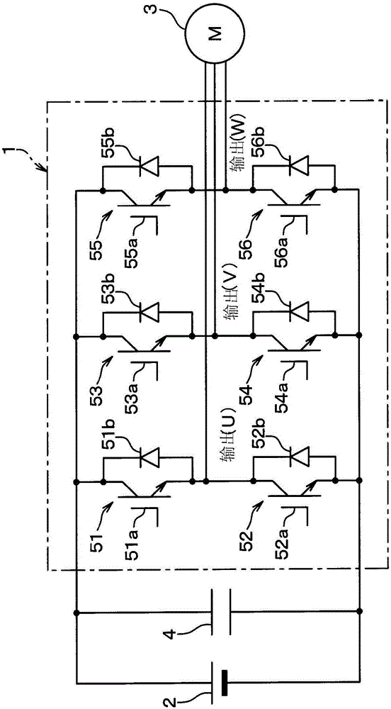
[0069] First, refer to figure 1 The configuration of the three-phase inverter circuit 1 included in the semiconductor module will be described. Such as figure 1 As shown, the three-phase converter circuit 1 is used to drive a load 3 of a three-phase AC motor based on a DC power supply (external power supply) 2. A filter capacitor 4 is connected in parallel in the three-phase converter circuit 1 to reduce fluctuations during switching, suppress the influence of noise, and form a constant power supply voltage.

[0070] The three-phase converter circuit 1 adopts a configuration in which the upper and lower branches 51 t...


PUM


Abstract

A semiconductor module is provided with three-phase upper arms (51, 53, 55) and lower arms (52, 54, 56), heat-dissipating plates (11, 12), a main circuit-side bus bar, an output terminal-side bus bar, a control terminal (14), and a resin mold part (18). The output terminal-side bus bar has U-phase to W-phase wiring layers (133-135) layered and arranged facing each other interposed by an insulating layer (130), and U-W terminals (13c-13e) for electrically connecting each of the U-phase to W-phase wiring layers and a load. There are an even number of U-phase to W-phase wiring layers.

Description

[0001] Cross-references to related applications [0002] This indication is based on the Japanese application number 2014-91148 for which it applied on April 25, 2014, and uses the description content here. technical field [0003] The present disclosure relates to a semiconductor module including a semiconductor switching element. Background technique [0004] Patent Document 1 proposes a structure capable of reducing the influence of noise in a power conversion device including a semiconductor module. In this power conversion device, a structure is adopted in which the input / output terminals drawn from the semiconductor module, the control terminals, and the control board are connected with the shortest distance. Thereby, the inductance of the main circuit (main circuit inductance) via the input / output terminal and the control terminal path inductance via the control terminal can be reduced, and the influence of noise can be reduced. [0005] However, in the semiconducto...

Claims


Application Information

Patent Timeline
IPC IPC(8): H02M7/48
CPCH02M7/48H02M7/003H01L2924/181H01L2224/48247H01L2224/73265H01L2924/00014H01L23/051H01L23/3107H01L23/367H01L23/3735H01L23/4334H01L23/5385H01L23/13H01L23/5383H01L23/5384H01L24/48H01L25/072H01L25/18H01L2224/32225H01L2224/8384H01L2224/33181H01L2224/73215H01L2224/29034H01L24/29H01L24/32H01L24/33H01L2224/2612H01L2224/0603H01L2924/00012H01L2224/32245H01L2924/00H01L2224/05599H01L2224/45099H01L2224/85399H01L23/04H01L23/3121H01L23/3675H01L23/492H01L23/49838H01L2224/48091H01L2224/48106H01L2924/1203H01L2924/13055H01L2924/13091H02M7/5387H02P27/06
Inventor 石野宽渡边友和
Owner DENSO CORP
Why Eureka
Try Eureka