Semiconductor assembly pressure testing device and testing equipment

A pressure test and semiconductor technology, which is applied in the field of semiconductor component pressure test equipment and its test equipment, can solve the problems of low production capacity and high gas leakage rate, and achieve the effect of improving the tightness, improving the pressure leakage rate, and increasing the test accuracy

Active Publication Date: 2017-01-04
KING YUAN ELECTRONICS
View PDF5 Cites 10 Cited by
  • Summary
  • Abstract
  • Description
  • Claims
  • Application Information

AI Technical Summary

Problems solved by technology

However, this design can only test a single pressure chamber at a time during the pressure test. In addition, the case uses a quick connection and clip method, resulting in a high gas leakage rate and a relatively low production capacity.

Method used


Image

  • Semiconductor assembly pressure testing device and testing equipment
  • Semiconductor assembly pressure testing device and testing equipment
  • Semiconductor assembly pressure testing device and testing equipment

Examples


Embodiment Construction

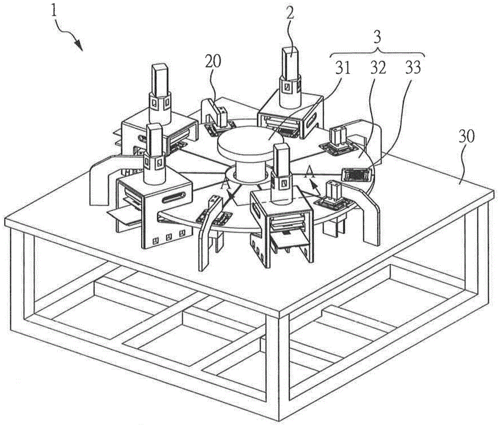
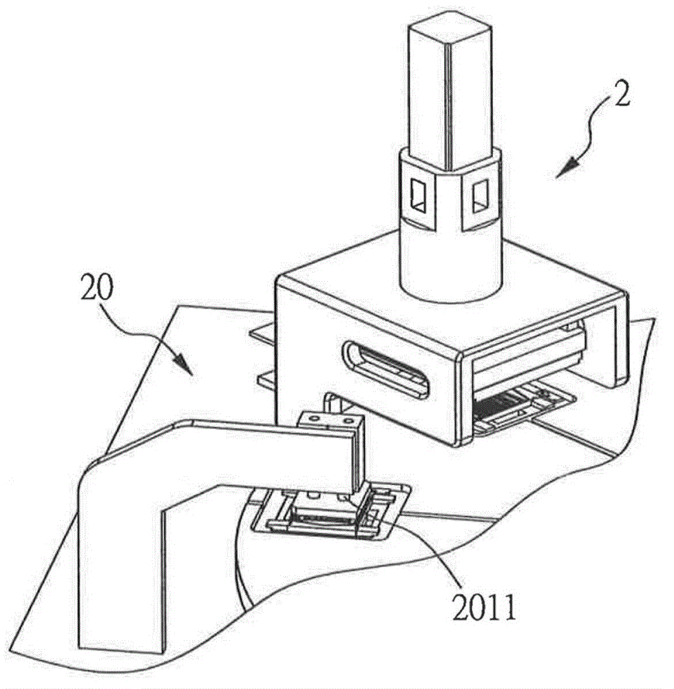
[0030] see figure 1 and figure 2, is a perspective view and an exploded view of a semiconductor component pressure testing device according to a preferred embodiment of the present invention. The figure shows a semiconductor component stress testing device 1, including a plurality of stress testing units 2, a plurality of preheating stations 20 and a turntable unit 3, each preheating station 20 and each stress testing unit 2 are arranged at intervals in a ring, In this embodiment, there are altogether five pressure testing units 2 and five adjacent preheating stations 20 , but the number is not limited thereto. figure 1 A group of pressure test units 2 is specially removed in order to describe some features of the turntable unit 3 conveniently.

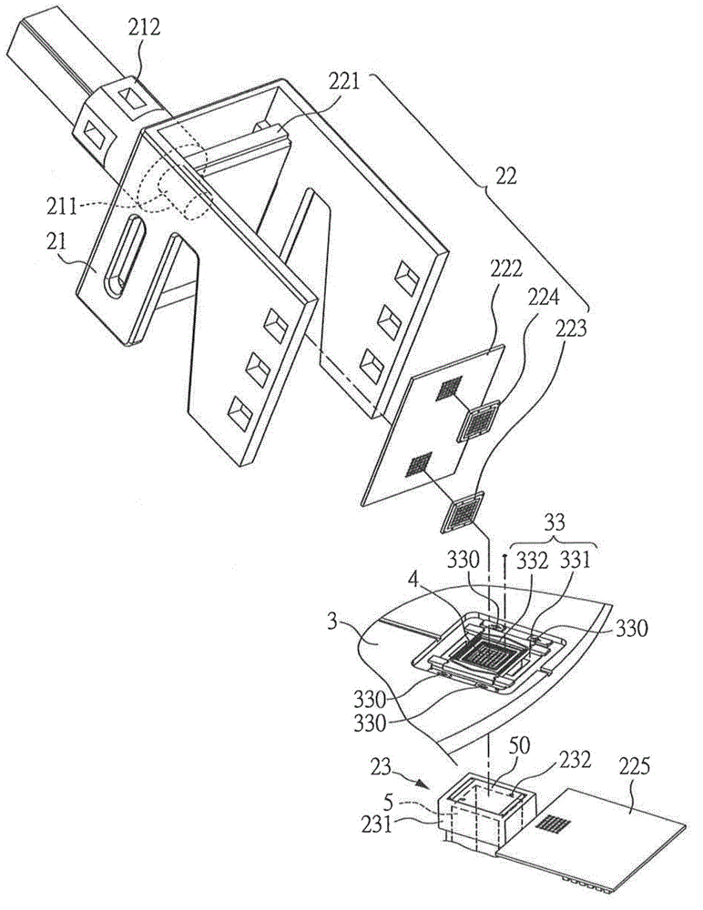
[0031] As shown in the figure, each pressure testing unit 2 includes a support frame 21 , an upper test seat 22 and a lower test seat 23 . The support frame 21 is fixed on a work table 30, and is equipped with a first power unit...


PUM


Abstract

The invention relates to a semiconductor assembly pressure testing device and testing equipment. The semiconductor assembly pressure testing device comprises a plurality of pressure testing units and a rotary plate unit. Each pressure testing unit comprises a support frame, an upper test base and a lower test base. The rotary plate unit comprises a pivot shaft, a rotary plate and a plurality of floating test bases, wherein each floating test base is connected with the rotary plate through a plurality of elastic pieces. The rotary plate rotates so as to impel each floating test base to be located between an upper test base and a lower test base correspondingly. The lower test base comprises a heating device and a heat conducting plate which are fixedly arranged on the lower test base. Each pressure testing unit supplies different test pressure and temperature so as to continuously test each semiconductor assembly in different temperature and pressure environments. Therefore, the semiconductor assembly testing device can be provided for a semiconductor assembly to be tested to be continuously transported and tested among a plurality of pressure testing units, thereby significantly improving the test capacity.

Description

technical field [0001] The invention relates to a semiconductor component pressure testing device and testing equipment thereof, in particular to a testing device and testing equipment suitable for testing the pressure sensing characteristics of a semiconductor component. Background technique [0002] Known technologies such as the semiconductor component stress testing device disclosed in U.S. Patent Publication No. 2009 / 0015277 A1, please refer to Figure 8 , is a side view of a known semiconductor component stress testing device. As shown in the figure, the pressure testing device described herein includes a first half cavity 91 and a second half cavity 92, wherein the first half cavity 91 is a fixed end, and the second half cavity 92 is lifted by a The device 90 moves vertically up and down to seal or separate the pressure testing device. The first half-cavity 91 has a lower groove 95 for carrying a carrier plate 97 on which a semiconductor component 96 is installed. T...

Claims


Application Information

Patent Timeline
Patent Type & Authority Applications(China)
IPC IPC(8): G01R31/26
Inventor 丁伟修陈文如
Owner KING YUAN ELECTRONICS
Why Eureka
Try Eureka