Digital chip function verifying method and system

A technology for digital chips and functional verification, applied in electrical digital data processing, special data processing applications, instruments, etc., can solve problems such as low verification accuracy, achieve comprehensive verification, and improve accuracy and reliability.

Inactive Publication Date: 2017-01-04
XIDIAN UNIV
View PDF3 Cites 3 Cited by
  • Summary
  • Abstract
  • Description
  • Claims
  • Application Information

AI Technical Summary

Problems solved by technology

[0006] The purpose of the present invention is to overcome the shortcomings of the above-mentioned prior art, and provide a digital chip function verification method and system for solving the technical problem of low verification accuracy existing in the prior art

Method used


Image

  • Digital chip function verifying method and system
  • Digital chip function verifying method and system
  • Digital chip function verifying method and system

Examples


Embodiment Construction

[0031] The present invention will be further specifically described below in conjunction with the accompanying drawings.

[0032] Refer to attached figure 1 :

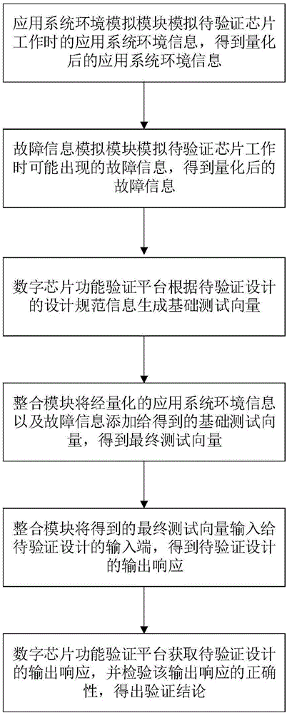
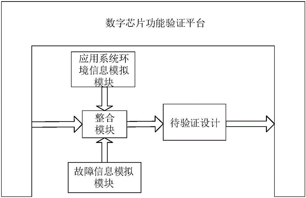
[0033] The digital chip function verification method of the present invention simulates its real system environment and the impact of fault information on the ideal stimulus received by the interface through certain methods and software simulations, and integrates the signal integrity problems brought about by the system environment information and fault information Into the basic test vector, so as to verify the correctness of timing and function of the design to be verified (DUV) with the test vector containing system environment information and fault information, the specific steps are as follows:

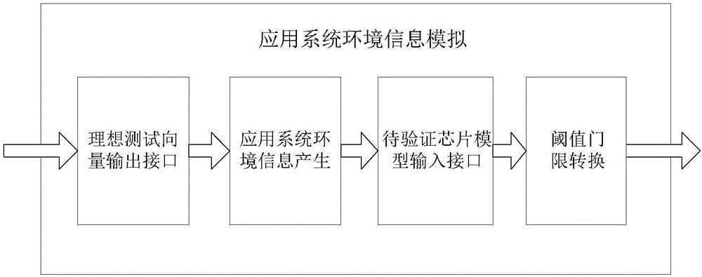
[0034] Step 1. The application system environment simulation module simulates the application system environment information when the chip to be verified works, and obtains the quantified application system environment ...


PUM


Abstract

The invention provides a digital chip function verifying method and system, and is used for solving the technical problems that verifying accuracy is low in the prior art. The environmental factor of an application system and influence of fault information to verifying results are considered. The verifying method comprises the following steps: simulating environmental information of the application system; simulating the fault information; generating a foundation test vector according to a design specification of a design to be verified; integrating the environmental information and the fault information with the foundation test vector; inputting the integrated vector to the design to be verified to obtain output response; and inputting the output response to a digital chip function verifying platform, and inspecting correctness of the output response to obtain verifying conclusions. The verifying system comprises a digital chip function verifying platform and the design to be verified, wherein the digital chip function verifying platform is connected with the design to be verified end to end, an output end of the digital chip function verifying platform is connected with an integrating module, an input end of the integrating module is connected with an application system environmental information simulating module and a fault information simulating module, and an output end of the integrating module is connected with an input end of the design to be verified.

Description

technical field [0001] The invention belongs to the field of digital chip verification, and relates to a digital chip function verification method and system considering application system environment factors and fault information, which can be used in the technical field related to digital chips. Background technique [0002] In integrated circuit design, design specifications describing chip functions and specification parameters are usually used as the starting point of design, and based on the design specifications, designers will then use hardware description languages ​​(HDL) such as Verilog and VHDL, at the register transfer level (RTL) Design is implemented at this level of abstraction. Design results are usually presented in the form of HDL code, which describes how the chip manipulates data so that data can flow correctly between the input, output, and clock registers of the circuit. After the chip design is completed, it must be verified. The main task of chip ve...

Claims


Application Information

Patent Timeline
Patent Type & Authority Applications(China)
IPC IPC(8): G06F17/50
CPCG06F30/20G06F30/398
Inventor 史江义李钊缪磊马佩军古生霖舒浩
Owner XIDIAN UNIV
Why Eureka
Try Eureka