Method of realizing photoetching of rewiring metal layer

A metal layer and rewiring technology, which is applied in the field of rewiring metal layer lithography, can solve the problem of low yield rate of rewiring metal layer, and achieve the effect of eliminating air bubbles, improving quality and reducing viscosity

Active Publication Date: 2017-01-04
SEMICON MFG INT (SHANGHAI) CORP
View PDF4 Cites 3 Cited by
  • Summary
  • Abstract
  • Description
  • Claims
  • Application Information

AI Technical Summary

Problems solved by technology

[0005] However, with the further increase of the process node, the yield rate of the redistribution metal layer formed by the existing technology is low

Method used


Image

  • Method of realizing photoetching of rewiring metal layer
  • Method of realizing photoetching of rewiring metal layer
  • Method of realizing photoetching of rewiring metal layer

Examples


Embodiment Construction

[0026] As mentioned in the background, with the further increase of the process node, the yield rate of the redistribution metal layer formed in the prior art is low.

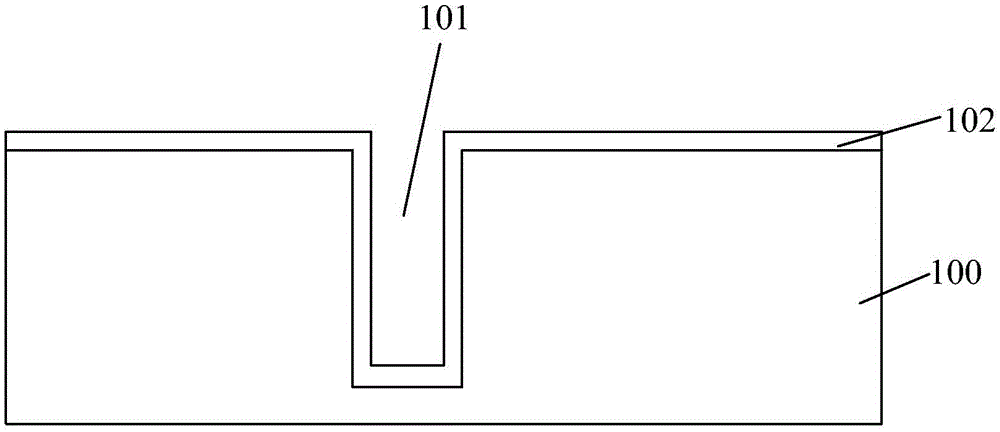
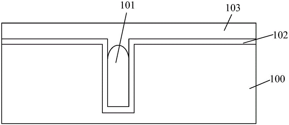
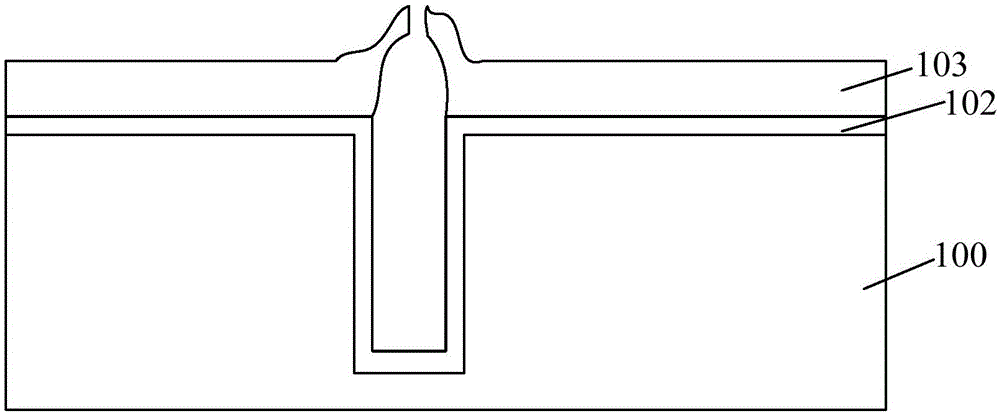
[0027] After further research, it was found that the low yield rate of the rewiring metal layer was mainly caused by the photoresist layer used to transfer the rewiring pattern. Specifically, please refer to figure 2 and image 3 , as the process node further increases, the size of the silicon hole 101 formed in the silicon wafer 100 becomes smaller and smaller. When the photoresist 103 is spin-coated on the surface of the silicon wafer 100, if the spin-coated photoresist is thinner, it is difficult to As a mask for subsequent etching to form the rewiring metal layer; if the photoresist that is spin-coated is thicker, it is difficult to completely fill the silicon hole 101 due to its high viscosity, and the photoresist is deposited on the top of the silicon hole 101. It is difficult to enter the bottom of th...


PUM

PropertyMeasurementUnit
thicknessaaaaaaaaaa
depthaaaaaaaaaa
thicknessaaaaaaaaaa

Abstract

The invention discloses a method of realizing photoetching of a rewiring metal layer. The method comprises steps: a semiconductor substrate is provided, wherein a hole passing through the partial thickness is formed in the semiconductor substrate, and the surface of the inner wall of the semiconductor substrate and the hole is coated with a metal layer; spin coating of a photoresist is carried out on the surface of the semiconductor substrate; the spin-coating photoresist is processed to enable the photoresist to fill the hole; after the photoresist fills the hole, soft baking, exposure, development and hard baking are carried out, and a patterned photoresist layer is formed; and with the patterned photoresist layer as a mask, the metal layer is etched to form a rewiring metal layer. bubbles formed in the hole when spin coating of the photoresist is carried out are eliminated, the quality of the formed patterned photoresist layer is improved, the yield of the subsequently-formed rewiring metal layer is high, and the yield of semiconductor products is high.

Description

technical field [0001] The invention relates to the technical field of semiconductor manufacturing, in particular to a method for realizing rewiring metal layer photolithography. Background technique [0002] During the formation of semiconductor devices, photolithography is usually used to transfer the mask pattern on the mask plate to the photoresist layer on the surface of the semiconductor device, and then transfer the mask pattern from the photoresist layer to the semiconductor device through the etching process. middle. Wherein, the redistribution (RDL) process of the prior art includes: [0003] Please refer to figure 1 , providing a silicon wafer 100, the silicon wafer 100 is formed with a silicon hole 101 through its partial thickness, and the surface of the silicon wafer 100 and the silicon hole 101 is covered with a metal layer 102; [0004] Please refer to figure 2 , spin coating photoresist 103 on the surface of the silicon wafer 100; afterward, steps such ...

Claims


Application Information

Patent Timeline
Patent Type & Authority Applications(China)
IPC IPC(8): H01L21/027H01L21/3213
CPCH01L21/0274H01L21/32136
Inventor 刘尧陈福成
Owner SEMICON MFG INT (SHANGHAI) CORP
Why Eureka
Try Eureka