White light QLED device based on quantum well structural quantum dots and preparation method
A quantum dot luminescence and quantum dot technology, which is applied in semiconductor/solid-state device manufacturing, electric solid-state devices, semiconductor devices, etc., can solve problems such as low luminous efficiency, complex structure, white light color coordinate drift, etc., and achieve simple device structure, reduce Loss, improve the effect of white light color coordinate drift
- Summary
- Abstract
- Description
- Claims
- Application Information
AI Technical Summary
Problems solved by technology
Method used
Image
Examples
preparation example Construction
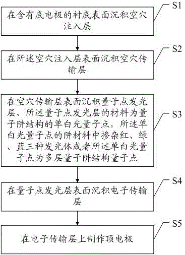
[0038] The present invention also provides a preferred embodiment of a preparation method for a white light QLED device based on quantum dots with a quantum well structure, such as figure 2 As shown, it includes the steps:
[0039] S1, depositing a hole injection layer on the surface of the substrate containing the bottom electrode;
[0040] S2. Depositing a hole transport layer on the surface of the hole injection layer;
[0041]S3. Depositing a quantum dot light-emitting layer on the surface of the hole transport layer. The material of the quantum dot light-emitting layer is a single white light quantum dot with a quantum well structure, and the well material of the single white light quantum dot is doped with red, green, and blue three A luminescent body or the single white light quantum dot is a multilayer quantum well structure quantum dot;
[0042] S4. Depositing an electron transport layer on the surface of the quantum dot luminescent layer;
[0043] S5. Fabricating...
Embodiment 1
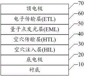
[0045] The white light QLED device includes from bottom to top: substrate, bottom electrode, hole injection layer (HIL), hole transport layer (HTL), quantum dot light emitting layer (EML), electron transport layer (ETL) and top electrode. Wherein, the substrate is a glass substrate, the bottom electrode is 120nm ITO, and the material of the HIL is PEDOT:PSS (20nm). The material of the HTL is TFB, and the thickness of the HTL is 45nm. The material of the EML is a three-layer quantum well structure quantum dot (ZnS / ZnSe:Ag, Cu, Mn / ZnS) with a thickness of 30 nanometers. The material of the ETL is nano zinc oxide, and the thickness of the ETL is 20nm. The material of the top electrode is Al.
Embodiment 2
[0047] The white light QLED device includes from bottom to top: substrate, bottom electrode, hole injection layer (HIL), hole transport layer (HTL), quantum dot light emitting layer (EML), electron transport layer (ETL) and top electrode. The substrate is a glass substrate, the bottom electrode is 120nm ITO, and the material of the HIL is PEDOT:PSS (20nm). The material of the HTL is TFB, and the thickness of the HTL is 45nm. The material of the EML is ZnS / ZnSe:Mn / ZnS / ZnSe:Cu / ZnS / ZnSe:Ag / ZnS quantum dots with a seven-layer quantum well structure, and the thickness is 30 nanometers. The material of the ETL is nano zinc oxide, and the thickness of the ETL is 25nm. The material of the top electrode is Al.
PUM
 Abstract
Description
Claims
Application Information

