Digital image acquisition device and system of external transmission electron microscope

Active Publication Date: 2017-01-11
SOUTH CHINA UNIV OF TECH
View PDF5 Cites 1 Cited by
  • Summary
  • Abstract
  • Description
  • Claims
  • Application Information

AI Technical Summary

Problems solved by technology

[0004] The defects of the above-mentioned transmission electron microscope are: 1. the CCD camera is installed at the bottom of the transmission electron microscope, through the passage of the transmission electron beam, the high-energy transmission electron beam is easy to cause damage to the CCD image sensor in the CCD camera, and its service life is greatly reduced; 2. It is inconvenient to replace the CCD camera or CCD image sensor, and the relevant devices at the bottom of the transmission electron microscope need to be disassembled, and the maintenance cost is high
[0006] Although the CCD image sensor in this side-mounted CCD system is not in the path of the transmitted electron beam, thus avoiding damage caused by direct bombardment by the transmitted electron beam, the defect of this side-mounted CCD system is: the small fluorescent screen enters Or when exiting the transmitted electron beam path, due to the error of mechanical movement, it is impossible to return to the original position accurately, resulting in the relative position between the small fluorescent screen and the CCD image sensor is easy to change, in order to make t

Method used


Image

  • Digital image acquisition device and system of external transmission electron microscope
  • Digital image acquisition device and system of external transmission electron microscope
  • Digital image acquisition device and system of external transmission electron microscope

Examples


Example Embodiment

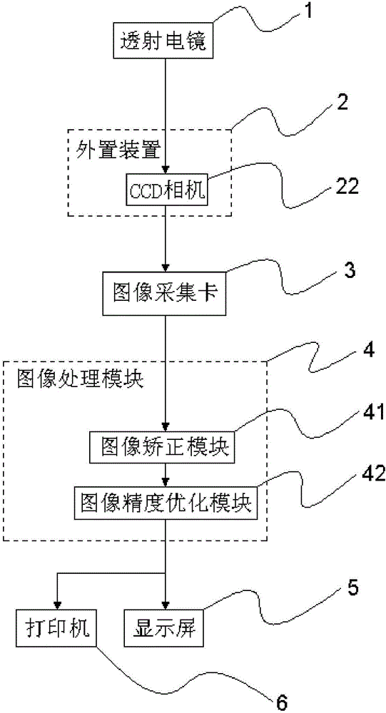
[0026] See image 3 , Which is a schematic diagram of signal transmission of the external transmission electron microscope image digital acquisition system of the present invention. The external transmission electron microscope image digital acquisition system of the present invention includes a transmission electron microscope 1, an external transmission electron microscope image digital acquisition device 2 (hereinafter referred to as an external device), an image acquisition card 3, an image processing module 4, a display screen 5 and a printer 6. . The external device 2 is installed on the transmission electron microscope 1, the external device 2, the image capture card 3, and the image processing module 4 are electrically connected in sequence, and the image processing module 4 is electrically connected to the display 5 and the printer 6 at the same time.

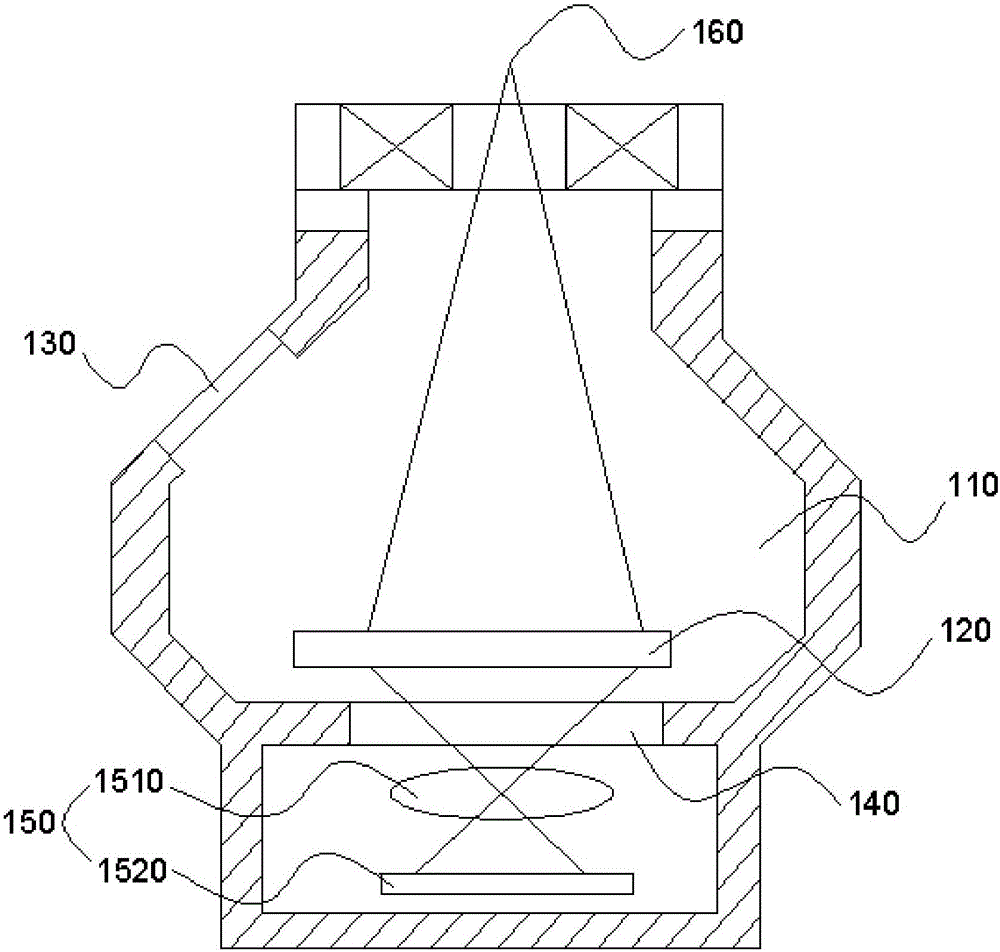
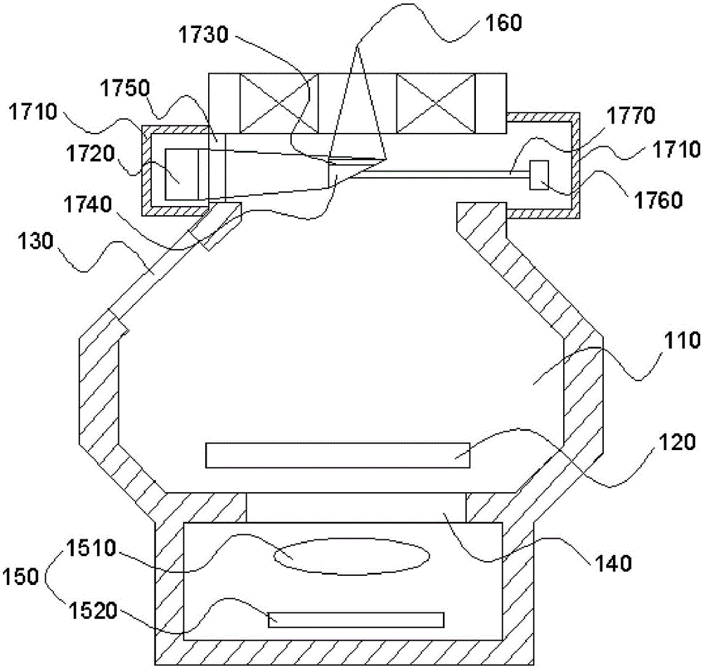
[0027] See Figure 4 , Which is a schematic diagram of the external device and the transmission electron microscope of...


PUM


Abstract

The invention discloses a digital image acquisition device of an external transmission electron microscope. The digital image acquisition device comprises an external shell and a CCD camera, wherein an opening is formed in at least one side of the external shell; the CCD camera is arranged at an open end of the external shell; the CCD camera converts a photosignal into an electric signal; and the external shell is detachably fixed outside an observation window of the transmission electron microscope. According to the digital image acquisition device of the external transmission electron microscope, the CCD camera is arranged outside the observation window and is arranged outside a transmission electron beam path and a bottom CCD system does not need to be used, so that the defects that the bottom CCD system is bombarded by electrons and easily damaged in the transmission electron beam path in the prior art are avoided. Meanwhile, if the CCD camera is damaged, one external device is replaced, so that the problem that maintenance is troublesome due to the fact that components of the transmission electron microscope need to be dismantled when the CCD camera is replaced in the prior art is solved. Furthermore, the external device disclosed by the invention is suitable for various models of transmission electron microscopes.

Description

Technical field [0001] The invention relates to an image acquisition device and system, in particular to a transmission electron microscope image digital acquisition device and system. Background technique [0002] Transmission electron microscope, referred to as transmission electron microscope, its basic working principle is as follows: the electron beam emitted by the electron gun passes through the condenser along the optical axis of the lens body in the vacuum channel, and converges it into a sharp, bright and uniform beam through the condenser The light spot is irradiated on the sample in the sample chamber; the electron beam after passing through the sample carries the structural information inside the sample, the amount of electrons passing through the dense part of the sample is small, and the amount of electrons passing through the sparse part is more; the convergence adjustment of the objective lens After focusing and primary magnification, the electron beam enters the...

Claims


Application Information

Patent Timeline
IPC IPC(8): H01J37/22
CPCH01J37/22H01J37/222
Inventor 戚其丰崔洁杨贤锋吴东晓尹诗衡杨辑刘金超
Owner SOUTH CHINA UNIV OF TECH
Why Eureka
Try Eureka