Process method and device

A process method and process device technology, applied in the field of semiconductor process control, can solve problems such as difficult operation, poor process stability and repeatability, and achieve the effect of reducing operation difficulty, strong stability and repeatability, and saving human resources

Inactive Publication Date: 2017-01-11
BEIJING NAURA MICROELECTRONICS EQUIP CO LTD
View PDF5 Cites 9 Cited by
  • Summary
  • Abstract
  • Description
  • Claims
  • Application Information

AI Technical Summary

Problems solved by technology

This has great operational difficulties for the existing scheme that relies entirely on craftsmen to manually modify the time parameters or power parameters of each proce

Method used


Image

  • Process method and device
  • Process method and device
  • Process method and device

Examples


Embodiment 1

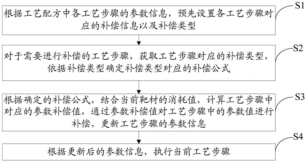
[0029] refer to image 3 , shows a flow chart of steps of a process method in Embodiment 1 of the present invention.

[0030] The processing method of the present embodiment comprises the following steps:

[0031] Step S1: According to the parameter information of each process step in the process formula, preset the compensation information and compensation type corresponding to each process step.

[0032]In this embodiment, first, the process recipe is preset. Specifically, the process recipe is configured with a plurality of process steps for performing a process on the substrate, and parameter information corresponding to the process steps. The parameter information corresponding to the process step can determine whether the target material is needed during the execution of the process step. If a process step requires a target during execution, it is necessary to preset compensation information and compensation type for the process step, and both the compensation informat...

Embodiment 2

[0052] refer to figure 2 , shows a flowchart of steps of a process method in Embodiment 2 of the present invention.

[0053] The processing method of the present embodiment specifically comprises the following steps:

[0054] Step S202: The semiconductor device acquires parameter information corresponding to the current process step in the set process recipe.

[0055] In this embodiment, those skilled in the art need to pre-set the compensation information and compensation type corresponding to each process step according to the parameter information of each process step in the process recipe. Specifically, the process recipe is configured with multiple process steps for processing the substrate and parameter information corresponding to the process steps.

[0056] Wherein, those skilled in the art can determine whether a target is needed during the execution of this process step through the parameter information corresponding to the process step. If a process step require...

Embodiment 3

[0104] refer to Figure 5 , shows a flow chart of steps of a process method in Embodiment 3 of the present invention.

[0105] In this embodiment, the process compensation method of the magnetic control PVD equipment is taken as an example to describe the process compensation method.

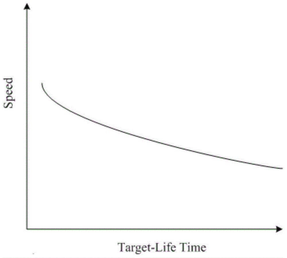
[0106] In this embodiment, a counter is set in the magnetron PVD equipment, and the counter is used to record the consumed life of the target. In this embodiment, the historical accumulated work done by the sputtering power supply on the target is used to represent the consumed life of the target. life.

[0107] Simultaneously, the setting format of a kind of preferred process formula is also provided in the present embodiment as shown in table 1:

[0108] Table 1

[0109] name Step1 Step2 …… Time(s) 10 5 …… Power(w) 100 500 …… Compensation Y N …… ComType Time power …… …… …… …… ……

[0110] By setting the above Recipe, that is, the p...


PUM


Abstract

The embodiment of the invention provides a process method and device. The method comprises the following steps of 1, setting compensation information and a compensation type which are corresponding to each process step in advance according to parameter information, in a process formula, of each process step; 2, acquiring the compensation type corresponding to the step with regard to the step needed to be compensated, and determining a compensation formula corresponding to the compensation type according to the compensation type; 3, calculating a parameter compensation value corresponding to the step by combining a current target consumption value according to the compensation formula, compensating the parameter value in the step according to the parameter compensation value, and updating the parameter information of the process step; and 4, executing the process step according to the updated parameter information. Through the process scheme provided by the embodiment of the invention, the process compensation is performed in real time by semiconductor equipment according to the configuration demand of the formula, and thus, the operation difficulty can be greatly reduced.

Description

technical field [0001] The invention relates to the technical field of semiconductor process control, in particular to a process method and device. Background technique [0002] With the rapid development of the semiconductor manufacturing industry, more and more semiconductor devices are produced and used, such as: magnetron PVD (Physical Vapor Deposition, physical vapor deposition) equipment, PLD (pulsed laser deposition, laser sputtering deposition) equipment, These semiconductor devices all need to use targets of corresponding materials when coating substrates. Such as figure 1 The structure diagram of a typical magnetron PVD equipment is shown, in which, 1 is the equipment cavity, 2 is the target used in sputtering deposition, the sputtering power supply outputs power to the target, 5 is the magnetron, and 3 is the base The film seat is used to contain the substrate, 4 is the substrate, the substrate seat can be driven by a motor or can be driven by a cylinder to move...

Claims


Application Information

Patent Timeline
IPC IPC(8): H01L21/66H01L21/67
CPCH01L21/67253H01L21/67207H01L22/20
Inventor 王晶
Owner BEIJING NAURA MICROELECTRONICS EQUIP CO LTD
Why Eureka
Try Eureka