New device for drying sample during micro nano device making process

A manufacturing process and new device technology, which are applied in semiconductor/solid-state device manufacturing, electrical components, circuits, etc., to achieve the effect of convenient use and strong operability

Inactive Publication Date: 2017-01-11
WUHAN UNIV OF TECH
View PDF3 Cites 0 Cited by
  • Summary
  • Abstract
  • Description
  • Claims
  • Application Information

AI Technical Summary

Problems solved by technology

[0003] The technical problem to be solved by the present invention is to provide an efficient and reliable way to obtain clean samples, thereby shortening the device manufacturing cycle for samples used in the manufacturing process of micro-nano devices, aiming at various pollution defects in the above-mentioned basic processing process of the prior art. New device for drying

Method used


Image

  • New device for drying sample during micro nano device making process
  • New device for drying sample during micro nano device making process
  • New device for drying sample during micro nano device making process

Examples


specific example

[0022] Specific examples, but without any limitation to the claims of the patent of the present invention, such as cleaning and drying of silicon carbide:

example 1

[0023] Example 1, the steps are as follows:

[0024] 1) The purchased silicon carbide is cut into a square with a side length of 2cm×2cm;

[0025] 2) cleaning the silicon carbide substrate;

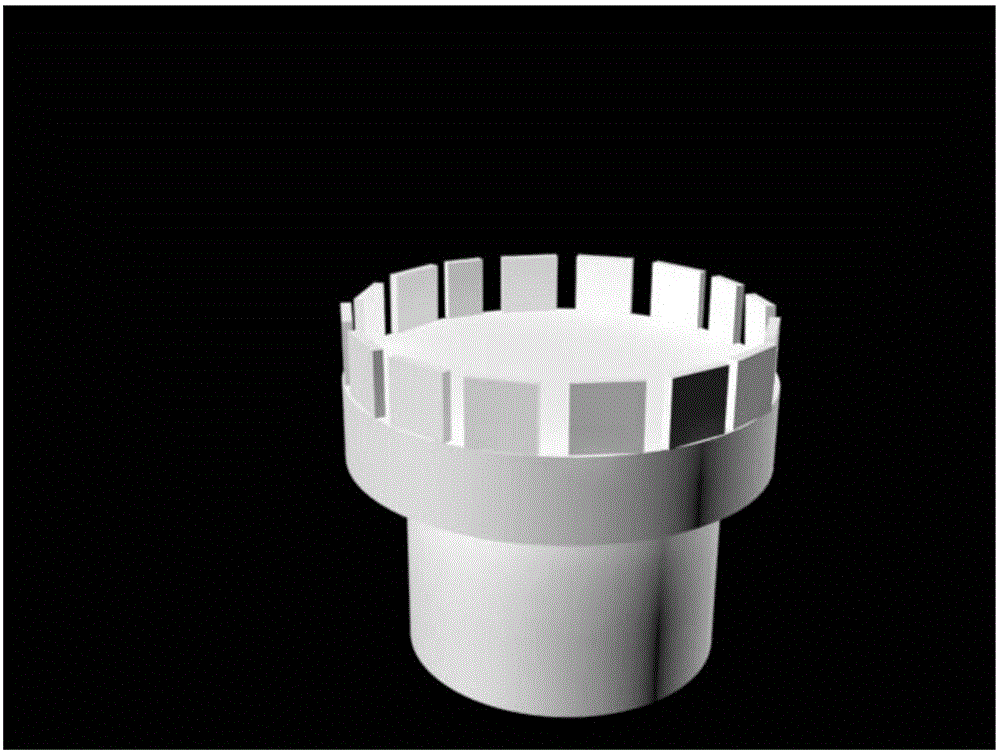
[0026] 3) Put the silicon carbide substrate ultrasonically cleaned in deionized water on a Teflon device for drying, and use the spin of the Teflon device to dry the substrate. The hollow tooth-shaped edge can not only hold the edge of the substrate to prevent the substrate from being thrown out at high speed, but also throw out the residual liquid on the substrate so that the substrate is not stained with liquid for the next drying operation .

example 2

[0027] Example 2, the steps are as follows:

[0028] 1) The purchased silicon substrate containing an oxide layer is cut into a square with a side length of 1.5cm×2cm;

[0029] 2) performing a cleaning operation on the silicon wafer;

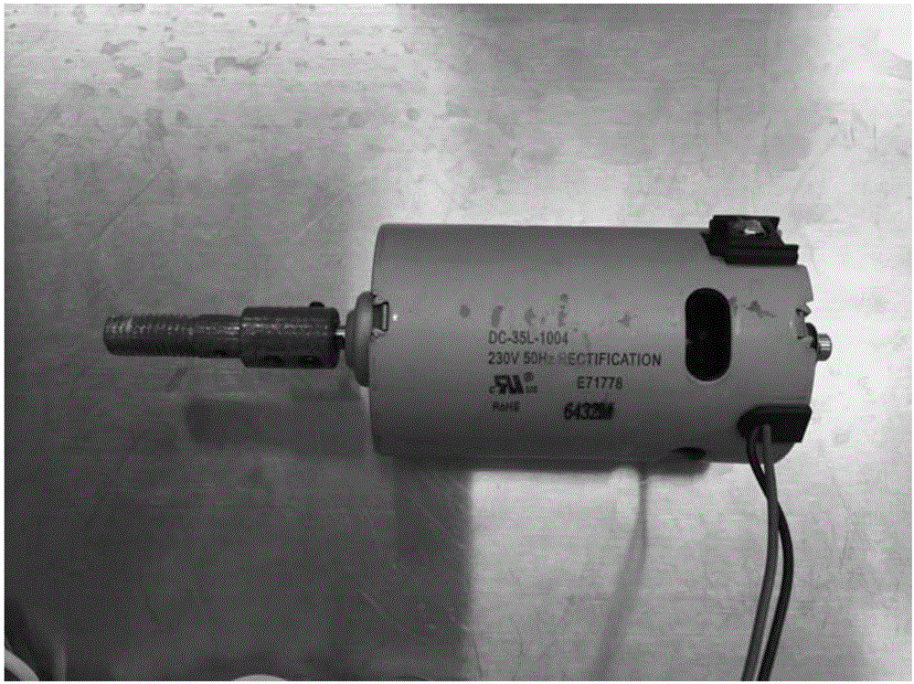
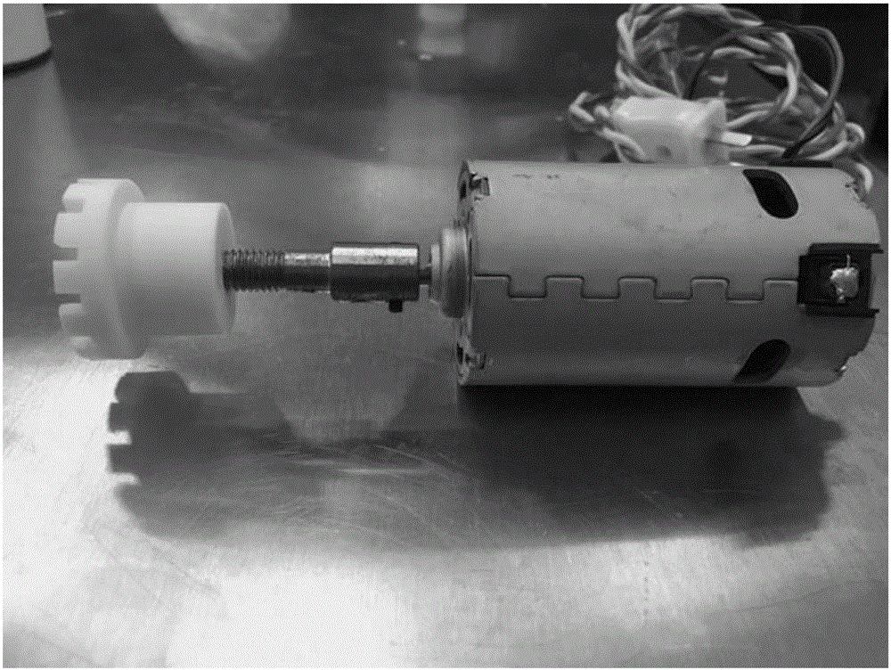
[0030] 3) Place the silicon wafer after ultrasonic cleaning in deionized water on the Teflon device for drying, and use the spin of the Teflon device to dry the substrate (it can be assembled with a small motor). The hollow tooth-shaped edge can not only hold the edge of the substrate to prevent the substrate from being thrown out at high speed, but also throw out the residual liquid on the substrate so that the substrate is not stained with liquid for the next drying operation .


PUM


Abstract

The invention relates to a new device for drying a sample during a micro nano device making process. The new device is characterized by comprising a Teflon device for drying; the Teflon device is internally provided with a groove, and the edge is provided with tooth-shaped disc-shaped Teflon. The whole set of Teflon device and the whole set of process are simple and convenient in operation, low in price, practical and is applicable to samples of various sizes and various types.

Description

technical field [0001] The patent of the present invention relates to a complete set of Teflon device for sample processing, more specifically, a complete set of new device for drying samples in the process of manufacturing micro-nano devices. Background technique [0002] At present, in the micromachining process of monocrystalline silicon, silicon carbide, substrates containing oxide layers, glass substrates and ceramic substrates, all external media in contact with the substrate are possible sources of impurities on the substrate. This mainly includes the following aspects: substrate pollution during processing and molding, environmental pollution, water pollution, reagent pollution, industrial gas pollution, process itself pollution, human body pollution, etc. In the production of semiconductor devices, the substrate must be strictly cleaned, otherwise the slight pollution on it will cause the device to fail. The purpose of cleaning is to remove contamination and impuri...

Claims


Application Information

Patent Timeline
Patent Type & Authority Applications(China)
IPC IPC(8): H01L21/67
CPCH01L21/67034
Inventor 何亮熊彪麦立强郝志锰
Owner WUHAN UNIV OF TECH
Why Eureka
Try Eureka