Integrated LED device and preparing method thereof

A technology of LED devices and manufacturing methods, applied in the direction of electric solid-state devices, semiconductor devices, electrical components, etc., can solve the problems of long etching time, low yield rate of ESD and IR, weak electrical connection, etc., and achieve structural and manufacturing process Simple, good electrical connection, and improved reliability

Inactive Publication Date: 2017-01-11
FOCUS LIGHTINGS SCI & TECH
View PDF18 Cites 2 Cited by
  • Summary
  • Abstract
  • Description
  • Claims
  • Application Information

AI Technical Summary

Problems solved by technology

[0009] The trench is deep (usually 4-7μm), the etching time is long, and the cost is high;
[0010] In order to ensure effective electrical insulation, a thicker insulating coating film must be deposited. Due to incomplete coating or poor film compactness, the ESD and IR yields will be low. At the same time, the deposition time of thick insulatin

Method used


Image

  • Integrated LED device and preparing method thereof
  • Integrated LED device and preparing method thereof
  • Integrated LED device and preparing method thereof

Examples


Embodiment Construction

[0045] In order to enable those skilled in the art to better understand the technical solutions in the present invention, the technical solutions in the embodiments of the present invention will be clearly and completely described below in conjunction with the drawings in the embodiments of the present invention. Obviously, the described The embodiments are only some of the embodiments of the present invention, not all of them. Based on the embodiments of the present invention, all other embodiments obtained by persons of ordinary skill in the art without making creative efforts shall fall within the protection scope of the present invention.

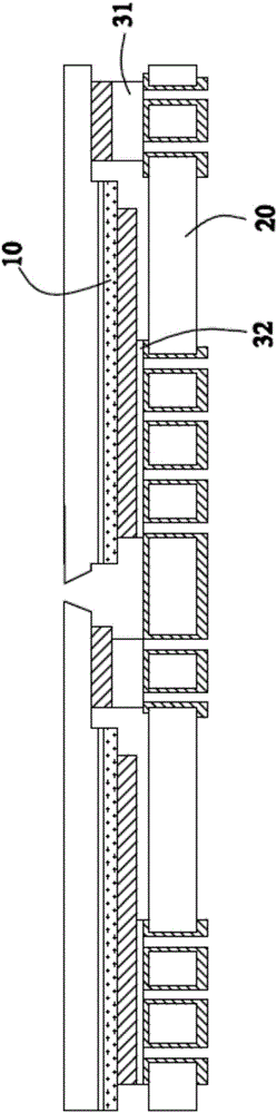
[0046] ginseng figure 1 As shown, the integrated LED device in the first embodiment of the present invention includes a patterned LED chip 10 and a patterned substrate 20 for carrying the LED chip 10 . The LED chip 10 and the patterned substrate 20 will be described in detail below.

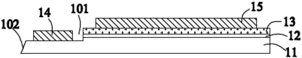
[0047] ginseng figure 1 and combine figure 2 As ...


PUM


Abstract

The invention provides an integrated LED device and preparing method thereof. The device comprises several LED chips. The LED chip contains N type semiconductor layer, multiple quantum well luminous layer, P type semiconductor layer, N electrode and P electrode. The N electrode connects N type semiconductor layer electrically, and the P electrode connects P type semiconductor layer electrically. The graphical substrate is used for carrying the LED chips and comprises several primary interconnected areas and secondary interconnected areas. The N electrode and P electrode in the LED chips respectively connect the primary interconnected areas and secondary interconnected areas in the graphical substrate electrically. The device connects the LED chips and graphical substrate electrically with simple structure and manufacturing technology improving the reliability of device and realizing the large power and high current.

Description

technical field [0001] The invention relates to the field of semiconductor chips, in particular to an integrated LED device and a manufacturing method thereof. Background technique [0002] A light-emitting diode (Light-Emitting Diode, LED) is a semiconductor electronic component that can emit light. This electronic component appeared as early as 1962. In the early days, it could only emit red light with low luminosity. Later, other monochromatic light versions were developed. Today, the light that can be emitted has covered visible light, infrared rays and ultraviolet rays, and the luminosity has also increased to a considerable extent. of luminosity. Because of its energy saving, environmental protection, safety, long life, low power consumption, low heat, high brightness, waterproof, miniature, shockproof, easy dimming, concentrated beam, easy maintenance, etc., it can be widely used in various indications, displays, decorations , backlight, general lighting and other f...

Claims


Application Information

Patent Timeline
IPC IPC(8): H01L25/075H01L33/00H01L33/62
CPCH01L25/0753H01L33/005H01L33/62
Inventor 王磊陈立人李庆
Owner FOCUS LIGHTINGS SCI & TECH
Why Eureka
Try Eureka