Novel high-performance light modulation thin film transistor based on quantum dot doped gate insulating layer

A technology of thin-film transistors and gate insulating layers, which is applied in the manufacture of transistors, semiconductor devices, semiconductor/solid-state devices, etc., can solve the problems of slow detection speed and loss of IGZO thin-film transistors, achieve simplified structure and preparation process, simple preparation process, good stability effect

Active Publication Date: 2016-05-04
SOUTHEAST UNIV
View PDF2 Cites 16 Cited by
  • Summary
  • Abstract
  • Description
  • Claims
  • Application Information

AI Technical Summary

Problems solved by technology

However, due to the insurmountable side effect of zinc oxide-based materials - light blocking effect, the detection speed of IGZO thin film transistors is extremely slow (tens of sec

Method used


Image

  • Novel high-performance light modulation thin film transistor based on quantum dot doped gate insulating layer
  • Novel high-performance light modulation thin film transistor based on quantum dot doped gate insulating layer
  • Novel high-performance light modulation thin film transistor based on quantum dot doped gate insulating layer

Examples


example 1

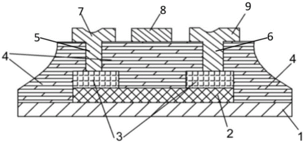
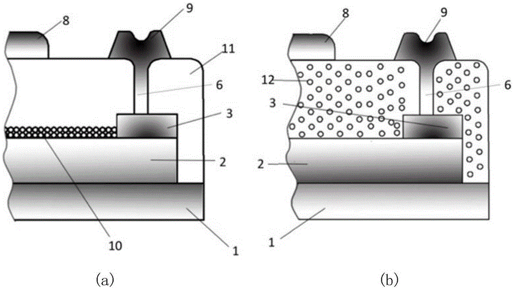
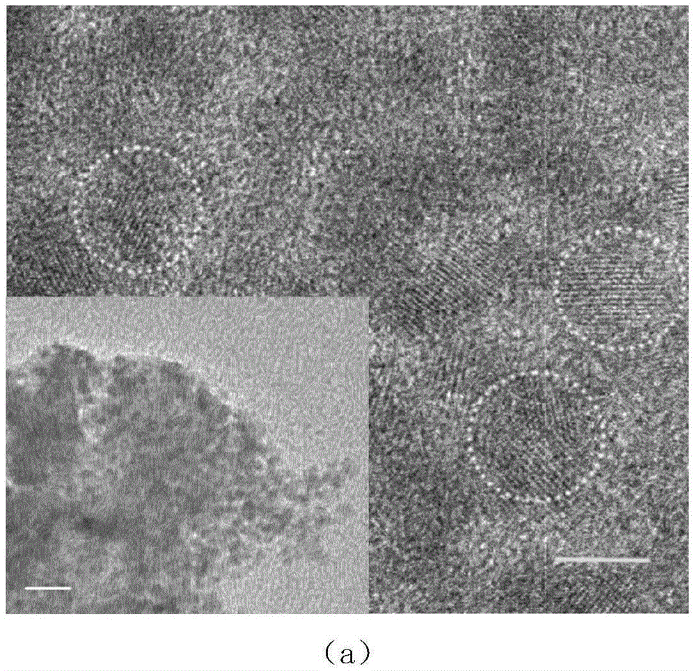
[0035] Example 1, the device structure is as figure 2 As shown in (a), the quantum dot layer 10 needs to be prepared first, so the process is as follows: a. Dissolve the solid quantum dot material in an ethanol solvent, and ultrasonicate for 15 minutes until the quantum dot nanoparticles are uniformly dispersed in ethanol. b. Spin-coat quantum dots on the glass substrate that has completed the process of step 1, select a spin-coating speed that accelerates from 1500 rpm to 1000 rpm, and set the spin-coating time to 30 seconds. c. Heating in air to 160° C. and annealing for 10 minutes to evaporate all remaining ethanol solution and form a quantum dot layer 10 of about 40 nm by thermal crosslinking at the same time. The particle size of the PbS quantum dots and the surface morphology of the film are as follows figure 2 (a) TEM picture shows. d. Continue to use the spin coating process to deposit Su8 photoresist on the substrate to wrap the formed quantum dot layer (process para...

example 2

[0036] Example 2, the structure is as figure 2 As shown in (b), it is necessary to mix and disperse Su8 organic photoresist and quantum dots in advance. Therefore, the process is as follows: a. Use an ultrasonic oscillator to ultrasonically stir at room temperature for 15 minutes so that the quantum dot material is evenly dispersed in the organic photoresist. In the mixed photoresist, too high concentration of quantum dots will lead to deterioration of the uniformity and insulation of the gate insulating layer. If the concentration is too low, the photoresponse characteristics of the photosensitive layer will be insufficient, so that the efficiency of the device will be low and it will not be able to generate sufficient photocurrent. Through our research, it is found that the quantum dot Su8 solution with a concentration of 1-3mg / ml can balance the performance of these two aspects. b. Spin-coat the Su8 photoresist mixed with PbS quantum dots onto the substrate. The specific ...


PUM

PropertyMeasurementUnit
Concentrationaaaaaaaaaa

Abstract

The invention discloses a novel high-performance light modulation thin film transistor based on a quantum dot doped gate insulating layer. A preparation method thereof comprises the following steps: depositing an active layer and a source and drain electrode contact layer on a base in sequence; spinning quantum dots and organic optical cement on the active layer to prepare the gate insulating layer; etching via holes for connecting the contact layer with active and drain electrodes on the gate insulating layer; and finally preparing a transparent electrode on the gate insulating layer, and etching the transparent electrode as the drain electrode, gate electrode and source electrode of a plane. Besides the three modulation electrodes of a traditional source and drain gate, the thin film transistor device disclosed by the invention can be taken as a fourth end modulation electrode through incident light. The light modulation thin film transistor with photoelectric detection and signal read functions is prepared by using the thin film transistor gate insulating layer doped with the quantum dots, so that the structure and preparation technology of the light modulation thin film transistor are greatly simplified, the dimensions of the device are shortened, and the photoelectric detection performance is improved.

Description

technical field [0001] The invention relates to an active layer / contact layer, a photosensitive gate insulating layer, a planar transparent source, drain and gate electrode structure and a preparation method thereof in a light modulating thin film transistor device. The thin film transistor not only has the traditional source and drain In addition to the three modulating terminal electrodes, the grid and the grid also have a modulation response characteristic to the incident light, so the incident light is used as the fourth light modulating terminal. Background technique [0002] At present, traditional photoelectric thin film transistors with light modulation function usually need to combine discrete photodetection elements and thin film transistors for electrical signal reading. On the one hand, this structure will cause a very complicated manufacturing process of the device, and the cost is high. On the other hand, traditional photodetection elements represented by phot...

Claims


Application Information

Patent Timeline
IPC IPC(8): H01L29/786H01L29/423H01L21/336
CPCH01L29/42364H01L29/42384H01L29/66742H01L29/786H01L29/78651
Inventor 刘向陶治陈静雷威伊曼纽尔·杰克塔耶·默罕默德
Owner SOUTHEAST UNIV
Why Eureka
Try Eureka