Organic light-emitting display device and manufacturing method thereof

A light-emitting display and manufacturing method technology, which is applied in semiconductor/solid-state device manufacturing, electrical components, electric solid-state devices, etc., can solve problems such as complicated process, difficult to realize, internal structure or etching affecting OLED performance, etc., to achieve low cost, Improve luminous efficiency and reduce internal reflection

Inactive Publication Date: 2017-01-11
TCL CHINA STAR OPTOELECTRONICS TECH CO LTD
View PDF5 Cites 11 Cited by
  • Summary
  • Abstract
  • Description
  • Claims
  • Application Information

AI Technical Summary

Problems solved by technology

These methods can improve the light extraction efficiency of OLED to a certain extent, but the process is complicated and difficult

Method used


Image

  • Organic light-emitting display device and manufacturing method thereof
  • Organic light-emitting display device and manufacturing method thereof
  • Organic light-emitting display device and manufacturing method thereof

Examples


Embodiment Construction

[0030] In order to make the object, technical solution and advantages of the present invention more clear, the present invention will be further described in detail below in conjunction with the accompanying drawings and embodiments. It should be understood that the specific embodiments described here are only used to explain the present invention, not to limit the present invention.

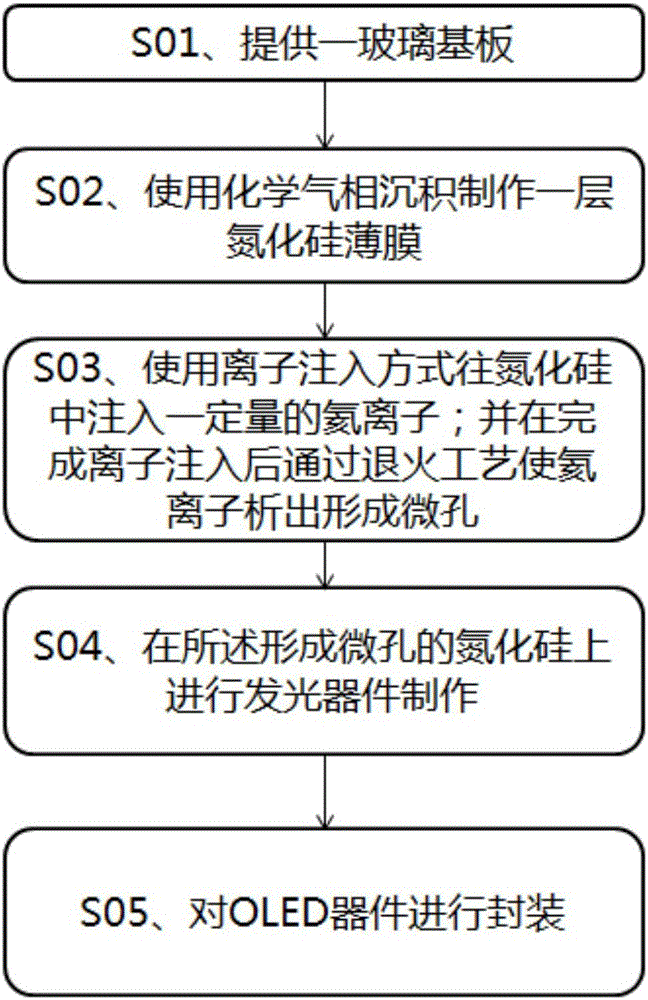
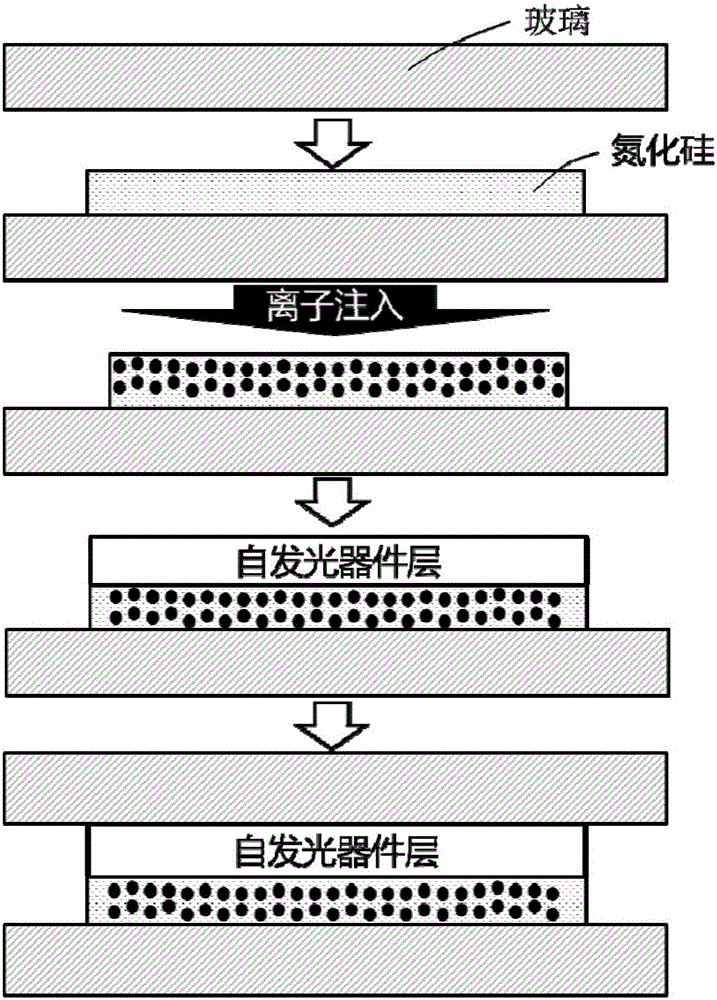
[0031] refer to figure 1 and figure 2 , the manufacturing process of the organic light-emitting display device of the present invention includes:

[0032] S01. Provide a glass substrate;

[0033] S02, making a layer of silicon nitride film on the glass substrate, preferably using chemical vapor deposition method to make;

[0034] S03, making micropores in the silicon nitride film;

[0035] S04, making OLED light-emitting devices on the silicon nitride film;

[0036] S05, packaging the OLED light emitting device.

[0037] Since the solid solubility of inert gas in silicon nitride is small,...


PUM

PropertyMeasurementUnit
Thicknessaaaaaaaaaa
Diameteraaaaaaaaaa

Abstract

The invention discloses an organic light-emitting display device, which comprises a lower substrate, a packaging layer, at least one light extraction layer, an electrode layer, a light-emitting layer and a functional layer, wherein the electrode layer, the light-emitting layer and the functional layer are arranged between the lower substrate and the packaging layer, and a micropore structure is formed in the light extraction layer. The invention further discloses a manufacturing method of the organic light-emitting display device. The organic light-emitting display device is provided with the light extraction layer with the micropore structure, and enables light to be scattered repeatedly by micropores when getting into the light extraction layer through reasonably setting the position of the light extraction layer, thereby reducing internal reflection at the light extraction layer on the whole, and enabling more light to be extracted and emitted from the light-emitting device. Therefore, the light-emitting efficiency of the device can be substantially improved. In addition, the organic light-emitting display device can be manufactured in a large scale, is low in cost and has important practical application values.

Description

technical field [0001] The present invention relates to the technical field of organic light-emitting semiconductor applications, in particular to an organic light-emitting display device and a manufacturing method thereof. Background technique [0002] OLED (Organic Light Emitting Display) and other self-luminous devices have the characteristics of self-illumination, wide viewing angle, long life, energy saving and environmental protection. With the rapid development of display and lighting industries, OLED has become an important hot spot in display design. [0003] Due to the influence of factors such as indium tin oxide (ITO) and glass substrate, various functional layers inside the organic light-emitting structure, glass substrate and air surface layer, reflection and refraction, about 80% of photons cannot escape into the air. , resulting in low photon utilization. In order to improve the light extraction efficiency of the device, researchers have proposed many method...

Claims


Application Information

Patent Timeline
IPC IPC(8): H01L51/50H01L51/52H01L27/32
CPCH10K59/00H10K50/00H10K50/85H10K50/854
Inventor 何超
Owner TCL CHINA STAR OPTOELECTRONICS TECH CO LTD
Why Eureka
Try Eureka