Optical device and fabrication thereof

a technology of optical devices and optical isolators, applied in the direction of laser optical resonator construction, laser details, optical resonator shape and construction, etc., can solve the problems of reducing performance and range, complex and costly, if not impossible, and complicating the procedures for reducing reflection back into the laser section, so as to achieve low internal reflex and good coupling efficiency

Inactive Publication Date: 2005-07-05
NORTHLIGHT OPTRONICS AB +1
View PDF19 Cites 2 Cited by
  • Summary
  • Abstract
  • Description
  • Claims
  • Application Information

AI Technical Summary

Benefits of technology

[0026]An advantage of the present invention is that low internal reflexes and a good coupling efficiency are simultaneously obtained.
[0027]Further characteristics of the invention and advantages thereof will be evident from the following detailed

Problems solved by technology

Low-chirp modulated laser sources are especially necessary in long-haul, high bit rate optical fiber transmission systems where chirp-induced pulse distortion reduces performance and range.
It is, however, complex and costly, if not impossible, to integrate an optical isolator with a laser and a modulator on a chip.
It is important to keep a good coupling efficiency in the arrangement, and this complicates the procedures for reducing reflections back into the laser section.
The suppression of internal reflexes of such a conventional device, however, is in many instances not sufficient, which results in poor yield in the fabrication of such integrated modulator / laser devices.

Method used


Image

  • Optical device and fabrication thereof
  • Optical device and fabrication thereof
  • Optical device and fabrication thereof

Examples


first embodiment

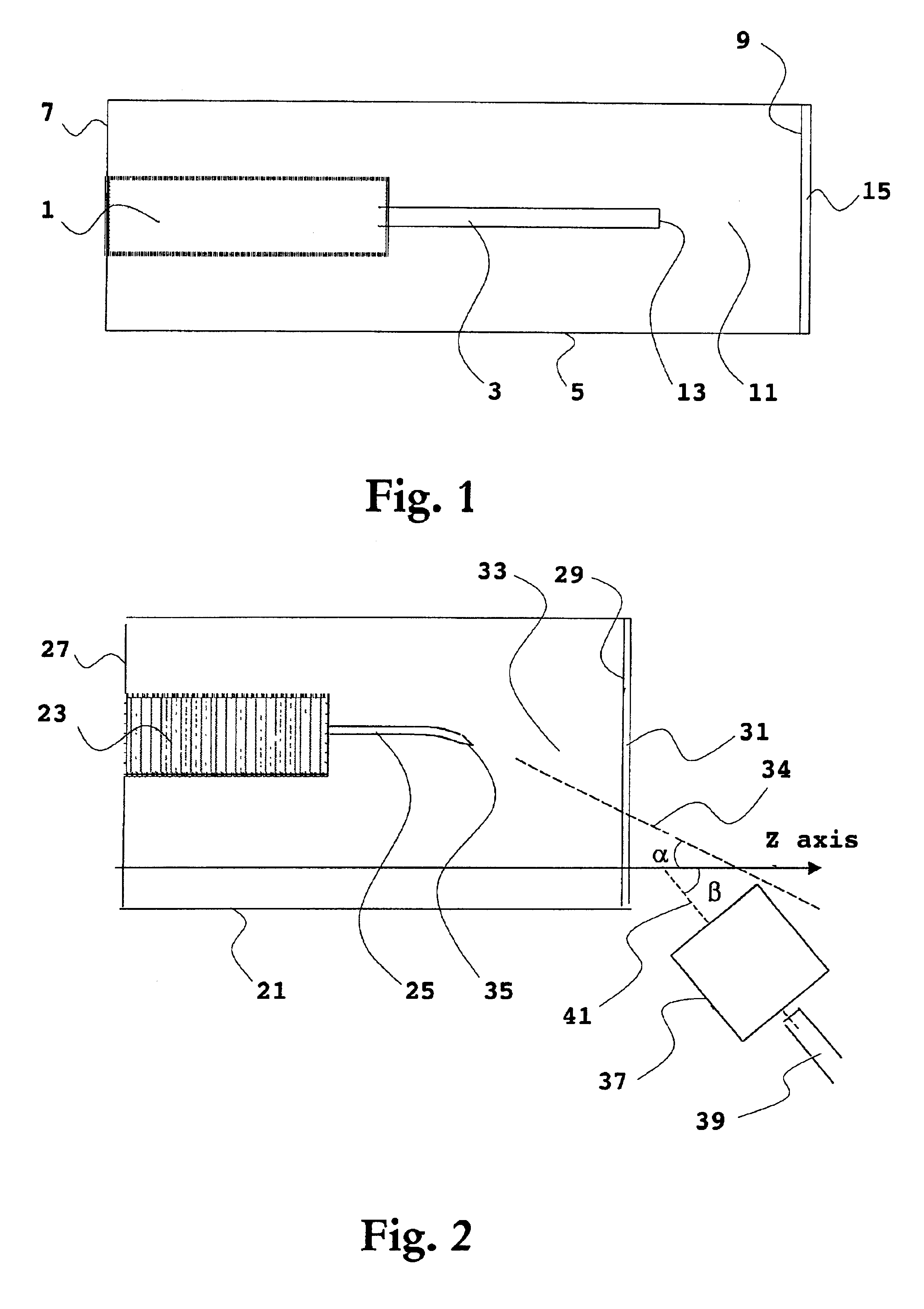
[0034]With reference to FIG. 2, which schematically illustrates a top view of an integrated laser / modulator device, the present invention will be depicted.

[0035]The integrated laser / modulator device comprises a substrate 21, in which a laser section 23 and a modulator section 25 are formed. The laser 23 is typically some kind of DFB (distributed feedback) laser, but may be any kind of suitable laser, e.g. a DBR (distributed Bragg reflection) laser. The modulator 25 is preferably an EAM (electro-absorption modulator), in which the waveguide has a bulk or a quantum well structure and the waveguide may be a buried or a ridge waveguide. Alternatively, the modulator is of other kind such as e.g. a Mach-Zehnder modulator.

[0036]The device is preferably fabricated in the material system InP / In1-xGaxAsyP1-y, but other material systems may be used.

[0037]Further, the device comprises a back facet 27 and a front facet 29 opposite to each other. Preferably, both facets are planar and parallel to...

second embodiment

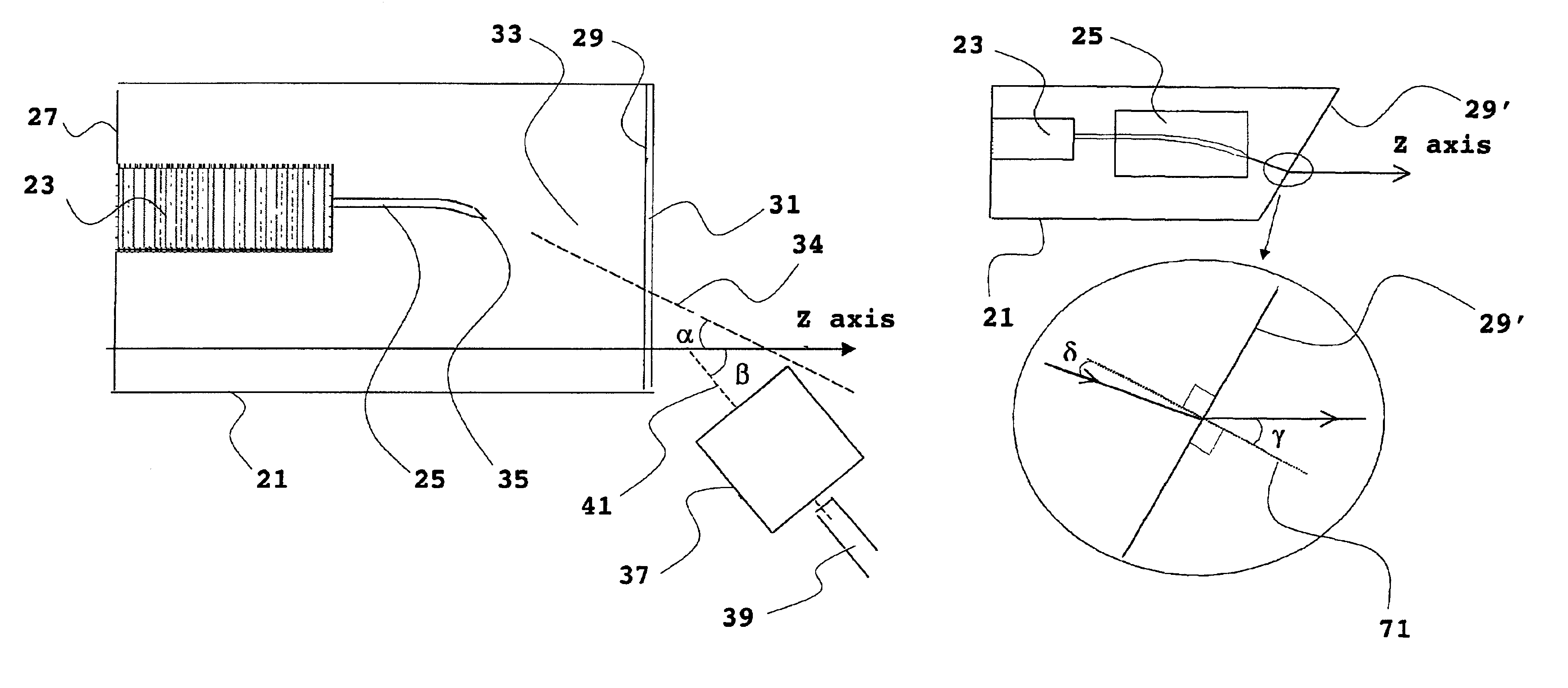
[0047]Next, with reference to FIG. 4, which is a schematic top view of an integrated laser / modulator device, wherein an enlargement of the front facet is shown in inset, the present invention will be depicted.

[0048]The device of this second embodiment is identical with the embodiment of FIG. 2 except that the device front facet, in FIG. 4 denoted 29′, is angled with respect to the Z axis instead of positioning any external out-coupling device at an angle with respect to the Z axis. All other parts of the device have the same reference numerals as they have in FIG. 1. Also in this embodiment an AR coating (not illustrated) may cover the front facet.

[0049]The front facet 29′ may be angled with respect to the Z axis by using any suitable technique such as e.g. dry etching. The angle γ of the dry-etched window termination is essentially given by Snell's law (to give an output coupling parallel with the Z axis).

[0050]It shall particularly be noted that in this embodiment one preferably u...


PUM


Abstract

An optical device has a back facet (27) and a front facet (29; 29′) opposite to each other, and includes a laser (23) adapted to emit light essentially perpendicular to said back facet; a modulator (25; 51; 55) having an input end and an output end (35; 53; 57), respectively, and adapted to receive and modulate light emitted from said laser and to output modulated light at said modulator output end; and a window region (33) arranged between said modulator output end and said device front facet, said device being further arranged such that modulated light output from said modulator is transmitted through said window region and is output from said device through said device front facet. The modulator is bent such that the modulated light output from said modulator is propagating essentially in a direction (34), which is angled (α; δ) with respect to the normal (Z; 71) of said device front facet.

Description

TECHNICAL FIELD OF THE INVENTION[0001]The present invention generally relates to the field of fiber optic communications. More specifically, the invention relates to an optical device comprising a laser and a modulator, and to a method for the fabrication of such optical device.DESCRIPTION OF RELATED ART AND BACKGROUND OF THE INVENTION[0002]In many fiber-optic systems application the demands on the light source are very stringent. Specifically, one needs good spectral purity in order to transmit high bit rate information over long distances. During laser modulation, a minimum level of spectral broadening necessarily occurs. Chirp, however, is an excess of spectral broadening beyond the spectral width required for modulation. Because different wavelengths propagate at different speeds in a dispersive medium, such as an optical fiber, the presence of significant chirp causes greater pulse spreading for a modulated optical signal transmitted across a fiber optic network.[0003]Thus, red...

Claims


Application Information

Patent Timeline
Patent Type & Authority Patents(United States)
IPC IPC(8): H01S5/00H01S5/026H01S5/10H01S5/12
CPCH01S5/0265H01S5/1085H01S5/12
Inventor GRANESTRAND, PERBJURSHAGEN, STEFANBJORKSTROM, .ANG.SALUNDQVIST, LENNART
Owner NORTHLIGHT OPTRONICS AB
Why Eureka
Try Eureka