Backboard processing method, adopted die and backboard manufactured by use of processing method

A processing method and backplane technology, applied in multilayer circuit manufacturing, printed circuit manufacturing, electrical components, etc., can solve the problem of inability to guarantee the position accuracy of the entry and exit surfaces, poor local fixation, and poor rivet fixation. problem, to achieve the effect of good flowering stability, increased rivet fixation, and uniform flowering

Active Publication Date: 2017-01-11
DONGGUAN SHENGYI ELECTRONICS
View PDF8 Cites 2 Cited by
  • Summary
  • Abstract
  • Description
  • Claims
  • Application Information

AI Technical Summary

Problems solved by technology

At present, fixed and evenly distributed rivets are used for conventional riveting, and the distance between the rivets is large. When making high-level multi-layer (more than 38 layers) large-scale (long side > 42 inches, inch is an imperial unit of length, 1 inch = 25.4mm) When the backboard is thick (thickness > 7mm), there is poor rivet fixing effect, which is prone to partial layer scrapping due to poor local fixing effect, especially during the moving process, each layer cannot be fixed and is easy to loose
Moreover, the existing drilling methods for backplanes with a thickness > 7mm cannot guarantee that the accuracy of the hole position on the entry surface and the exit surface can meet the requirements of backdrilling on the crimping and non-crimping surfaces of the backplate, thus resulting in crimping failure and backdrilling Residual copper causes short circuit
Based on the above reasons, the current high-layer and large-size thick backplane cannot meet the requirements of controlling the alignment within 7mil (mil, imperial length unit, 1mil=0.001 inch)

Method used


Image

  • Backboard processing method, adopted die and backboard manufactured by use of processing method
  • Backboard processing method, adopted die and backboard manufactured by use of processing method
  • Backboard processing method, adopted die and backboard manufactured by use of processing method

Examples


Embodiment Construction

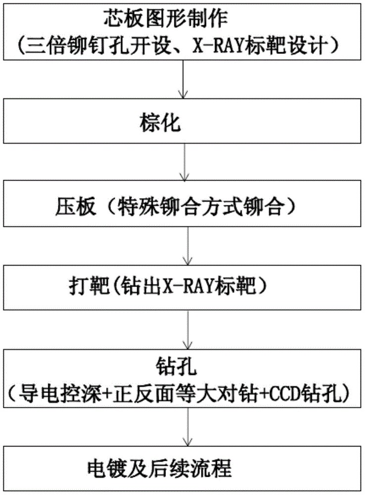
[0030] In order to explain in detail the technical solutions adopted by the present invention to achieve the intended technical purpose, the technical solutions in the embodiments of the present invention will be clearly and completely described below in conjunction with the accompanying drawings in the embodiments of the present invention. Obviously, the described implementation Examples are only part of the embodiments of the present invention, rather than all embodiments, and, on the premise of not paying creative work, the technical means or technical features in the embodiments of the present invention can be replaced, the following will refer to the accompanying drawings and combine Examples illustrate the present invention in detail.

[0031] see figure 1 , the present invention is a backplane processing method capable of improving the alignment of multi-layer large-size thick backplanes, comprising the following steps.

[0032] 1) Manufacturing of sub-core board graph...


PUM


Abstract

The invention provides a backboard processing method and an adopted die. The backboard processing method comprises following steps of: 1) manufacturing multiple sets of rivet holes and multiple target graphs in / on each sub core board, wherein each set of the rivet holes comprise at least three linearly arranged rivet holes; 2) browning the sub core boards; 3) laminating and riveting the sub core boards to form a backboard, wherein each set of the rivet holes are riveted to two rivet holes; 4) using a target drilling machine to grab target graphs on the backboard and drilling target holes in positions of the target graphs; and 5) using a CCD drilling machine to drill target holes so as to use the target holes as targets, and carrying out front-back face equal-size opposite drilling of functional holes on the backboard in a mode of conductive depth controlling. The method can improve the alignment precision control of the overlapping of all sub core boards in a manufacturing process of the backboard, and improves the machining precision and yield of the backboard.

Description

technical field [0001] The invention relates to a method for manufacturing a circuit board, in particular to a method for processing a multi-layer large-size thick backboard, a mold used, and a backboard prepared by the method. Background technique [0002] In the PCB industry, the backplane is a mainboard commonly used in electrical equipment. It is equipped with interfaces to facilitate the insertion of various types of substrates, such as computer motherboards, graphics cards, memory, hard drives, and CPUs are all plugged into the backplane. The backplane has powerful functions and is formed by stacking multiple sub-core boards. When the sub-core boards are stacked and combined, they are usually riveted by rivets. At present, fixed and evenly distributed rivets are used for conventional riveting, and the distance between the rivets is large. When making high-level multi-layer (more than 38 layers) large-scale (long side > 42 inches, inch is an imperial unit of length,...

Claims


Application Information

Patent Timeline
IPC IPC(8): H05K3/46
CPCH05K3/46H05K2203/166
Inventor 焦其正杜红兵王小平何平
Owner DONGGUAN SHENGYI ELECTRONICS
Why Eureka
Try Eureka