Energy interband non-local quantum tunneling simulation method with current conservation characteristic

A technology of quantum tunneling and simulation method, applied in the field of semiconductor device simulation, can solve the problems of numerical analysis error of device structure, not considering the overall tunneling current conservation on both sides, etc.

Active Publication Date: 2017-01-18
SHANGHAI INST OF SPACE POWER SOURCES
View PDF2 Cites 7 Cited by
  • Summary
  • Abstract
  • Description
  • Claims
  • Application Information

AI Technical Summary

Problems solved by technology

[0003] However, the above-mentioned non-local model still treats the point-to-point tunneling current as a compound item in the carrier continuity equation, and does not consider the conservation of the overall tunneling current on both sides, that is, the quantum tunneling current fr...

Method used


Image

  • Energy interband non-local quantum tunneling simulation method with current conservation characteristic
  • Energy interband non-local quantum tunneling simulation method with current conservation characteristic
  • Energy interband non-local quantum tunneling simulation method with current conservation characteristic

Examples


Embodiment 1

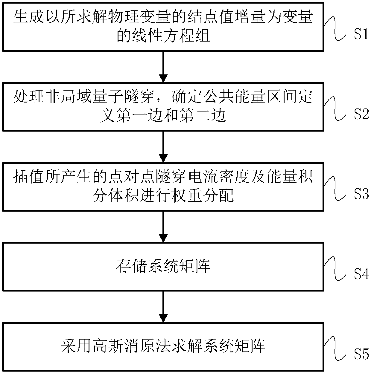
[0050] like figure 1 As shown, the present invention discloses Embodiment 1 of an inter-band nonlocal quantum tunneling simulation method with current conservation characteristics, and the method specifically includes the following steps:

[0051] S1. In the physical area of ​​discrete semiconductor devices, using partial differential equation numerical methods, such as finite volume method, finite difference method, and finite element method, etc., the generation of discrete semiconductor differential equations and boundary conditions takes the node value increment of the physical variable to be solved as a variable system of linear equations.

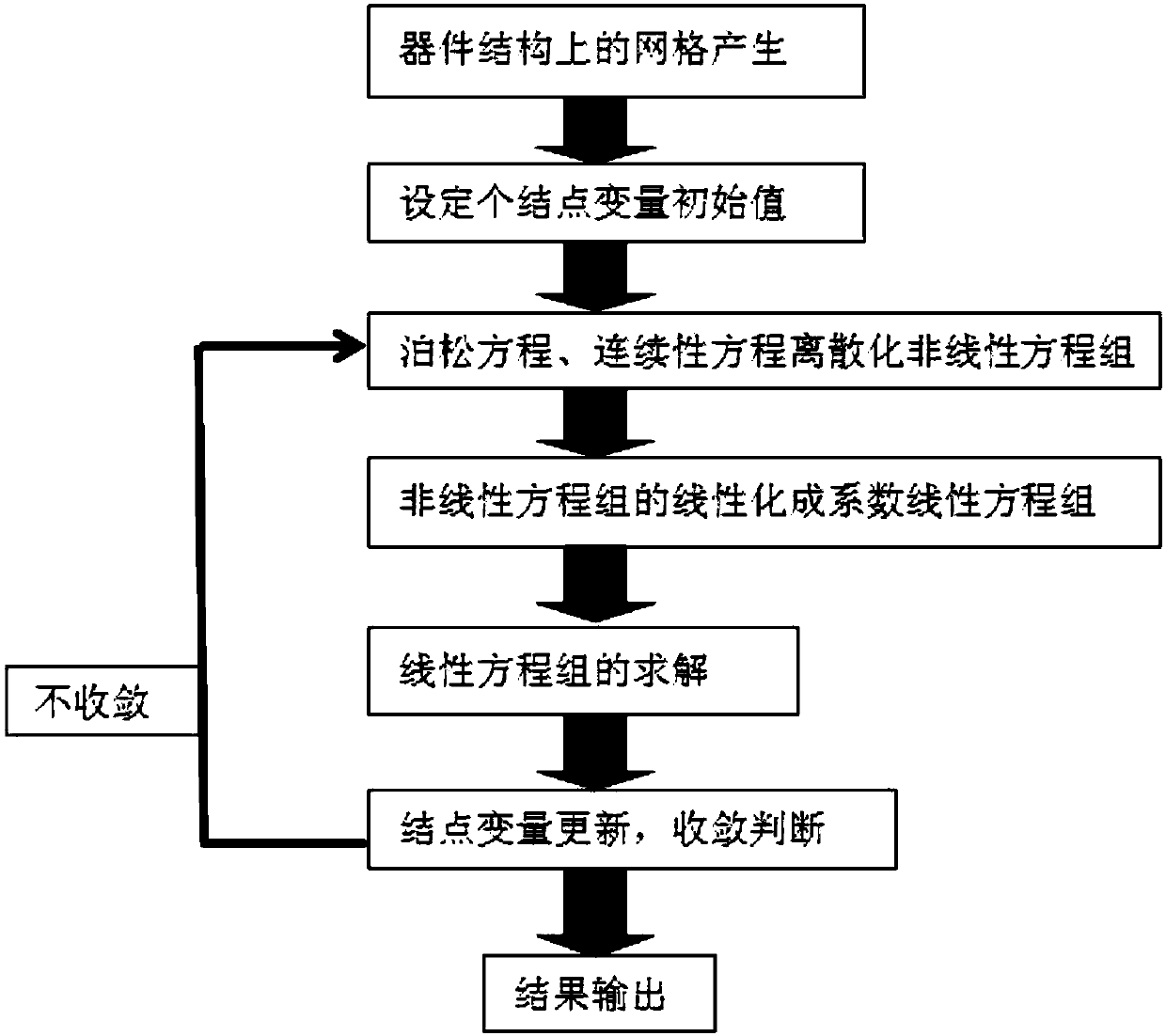
[0052] like figure 2 As shown in Fig. 1 , the general process of semiconductor device simulation includes: firstly, mesh generation is performed according to the geometric shape of the device structure. Secondly, based on the partial differential equation discretization method, the Poisson equation, electron and hole continuity equ...


PUM


Abstract

The invention discloses an energy interband non-local quantum tunneling simulation method with a current conservation characteristic. The method comprises the steps of generating a linear equation system which adopts a nodal value increment of a solved physical variable as a variable in a dispersing semiconductor device physical region; processing non-local quantum tunneling, determining a public energy zone for defining a first side and a second side; carrying out weight distribution on point-to-point tunneling current density and energy integral volume produced by interpolation; dividing a coefficient matrix of the linear equation system into a principal matrix caused by general differential equation dispersing and an additional coefficient matrix caused by non-local quantum tunneling with the current conservation characteristic, and storing; adopting a Gaussian origin eliminating method to solve the coefficient matrix. According to the energy interband non-local quantum tunneling simulation method with the current conservation characteristic provided by the invention, the non-local quantum tunneling current conservativeness is ensured, and the simulation error and the uncertainty brought by non-conservation are eliminated; by utilizing a method combining the principal matrix and an auxiliary incidence matrix, the coefficient linear equation system obtained through linearizing a non-linear equation system can be quickly solved, and the solving efficiency is improved.

Description

technical field [0001] The invention relates to a semiconductor device simulation method, in particular to a non-local quantum tunneling simulation method between energy bands with the characteristic of current conservation. Background technique [0002] Nonlocal quantum tunneling between different energy bands is a very common physical effect in compound semiconductor devices, which is common in many semiconductor devices, such as multi-junction solar cells and tunneling field effect transistors. How to accurately simulate this physical phenomenon is always concerned with semiconductor device physics and numerical mathematics. The usual method is to convert the point-to-point tunneling current density into a composite term of various continuity equations. The more commonly used is the Kane local model (E.O.Kane, "Zener tunneling in semiconductors", J.Phys.Chem.Solids, vol.12, pp.181-188, 1959), in this model, the energy band Non-local quantum tunneling is treated as a quan...

Claims


Application Information

Patent Timeline
IPC IPC(8): G06F17/50
CPCG06F30/20G06F2119/06
Inventor 张玮李欣益陆宏波陈杰张华辉杨丞张梦炎郑奕张建琴
Owner SHANGHAI INST OF SPACE POWER SOURCES
Why Eureka
Try Eureka