In-situ photoelectric multifunctional coupling atomic force microscope testing system
A technology of atomic force microscope and testing system, applied in the direction of control/regulation system, scanning probe microscopy, measuring device, etc. Independent and offline testing and other issues, to achieve the effect of accurate test results, convenient operation, stable and uniform airflow
Inactive Publication Date: 2017-01-25
SHENZHEN INST OF ADVANCED TECH CHINESE ACAD OF SCI +1
View PDF15 Cites 5 Cited by
- Summary
- Abstract
- Description
- Claims
- Application Information
AI Technical Summary
Problems solved by technology
[0004] The technical problem to be solved by the present invention is that the existing photoelectric testing system and the multi-functional probe atomic force microscope can only test separately, individually and offline, which cannot satisfy scientific researchers to perform in-situ, synchronous and real-time macroscopic performance testing and microstructural characterization of samples. combined requirements
Method used
View moreImage
Smart ImageViewing Examples

Examples
Embodiment
[0022] Embodiment: Under a certain temperature and pressure, the macroscopic photoelectric performance and microstructural information of the sample are tested using the in-situ optoelectronic multifunctional coupling atomic force microscope system, and the macroscopic photoelectric performance and microstructural information of the in-situ, synchronous and real-time sample device are obtained.
Login to View More PUM
| Property | Measurement | Unit |
|---|---|---|
| Wavelength | aaaaa | aaaaa |
| Light intensity | aaaaa | aaaaa |
Abstract
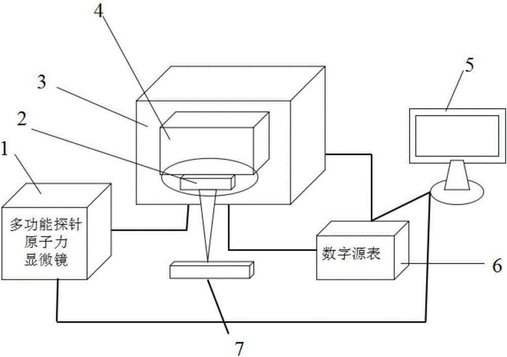
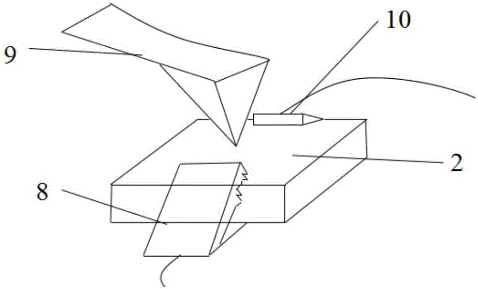
The invention discloses an in-situ photoelectric multifunctional coupling atomic force microscope testing system. The in-situ photoelectric multifunctional coupling atomic force microscope testing system comprises a light source and volt-ampere testing system of a photoelectric device, a multifunctional probe atomic force microscope system and an atmosphere protection system, wherein the light source and volt-ampere testing system of the photoelectric device comprises a fixture, a light source and a digital source meter; the multifunctional probe atomic force microscope system comprises a multifunctional probe, a laser emitter, a laser spot position detector, a laser detector, a data outgoing line and a computer display; the atmosphere protection system comprises a box, a gas inlet and outlet device, a spiral air current forming device, a temperature and humidity control device, a gas storage device, an occlusion design sliding door and an observing window. The testing system has the advantages that a photoelectric testing part and a multifunctional probe atomic force microscope are organically combined together in an integrated system, so that macroscopic photoelectric performance and microscopic information such as microscopic change information of electronics, ionization, polarization and the like of working samples can be tested synchronously in situ in real time.
Description
technical field [0001] The invention relates to a device for in-situ testing the macroscopic performance and microstructure of a photoelectric conversion device, in particular to an in-situ photoelectric multifunctional coupling atomic force microscope testing system. Background technique [0002] Atomic Force Microscope (AFM), an analytical instrument that can be used to study the surface structure of solid materials, including insulators. In 1986, Binnig collaborated with C.F. Quite of Stanford University and Christophe Gerber of IBM Zurich Laboratory to develop the atomic force microscope, which is a scanning probe microscope that does not require conductive samples {Phys. Rev. Lett., 1986, 56, 930-933}. It studies the surface structure and properties of substances by detecting the extremely weak interatomic interaction between the surface of the sample to be tested and a miniature force-sensitive element. One end of a pair of microcantilever sensitive to weak force is ...
Claims
Login to View More Application Information
Patent Timeline
 IPC IPC(8): G01Q60/24G01Q60/42G05D27/02
CPCG01Q60/24G01Q60/42G05D27/02
Inventor 赵晋津孔国丽刘正浩欧云贾春媚魏丽玉
Owner SHENZHEN INST OF ADVANCED TECH CHINESE ACAD OF SCI
Features
- R&D
- Intellectual Property
- Life Sciences
- Materials
- Tech Scout
- Unparalleled Data Quality
- Higher Quality Content
- 60% Fewer Hallucinations
Learn More Browse by: Latest US Patents, China's latest patents, Technical Efficacy Thesaurus, Application Domain, Technology Topic, Popular Technical Reports.
© 2025 PatSnap. All rights reserved.Legal|Privacy policy|Modern Slavery Act Transparency Statement|Sitemap|About US| Contact US: help@patsnap.com