Supercharge Your Innovation With Domain-Expert AI Agents!

Load modulation circuit of NFC tag compatible with amplitude limiting function

A load modulation and control circuit technology, which is applied to record carriers used in machines, instruments, computer components, etc., can solve the problems of increasing circuit design complexity, large size, and increased chip area, so as to reduce complexity and reduce chip size. area effect

Active Publication Date: 2017-02-01
中黍(北京)生物科技有限公司
View PDF3 Cites 0 Cited by
  • Summary
  • Abstract
  • Description
  • Claims
  • Application Information

AI Technical Summary

Problems solved by technology

The size of these load modulation tubes and limiter circuit control tubes connected across the two ends of the antenna is relatively large, so if this solution is used in the entire RF front-end circuit design, it will increase the design complexity of the circuit and give the chip The area brings additional increase, which increases the cost of the chip

Method used


Image

  • Load modulation circuit of NFC tag compatible with amplitude limiting function
  • Load modulation circuit of NFC tag compatible with amplitude limiting function
  • Load modulation circuit of NFC tag compatible with amplitude limiting function

Examples


Embodiment Construction

[0028] The present invention will be further described below in conjunction with specific embodiments, and the advantages and characteristics of the present invention will become clearer along with the description. However, these embodiments are only exemplary and do not constitute any limitation to the scope of the present invention. Those skilled in the art should understand that the details and forms of the technical solutions of the present invention can be modified or replaced without departing from the spirit and scope of the present invention, but these modifications and replacements all fall within the protection scope of the present invention.

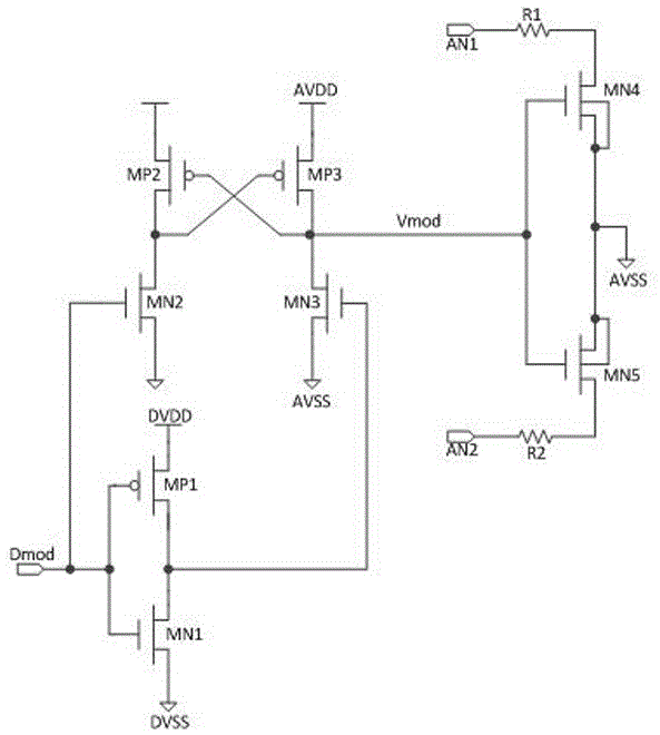
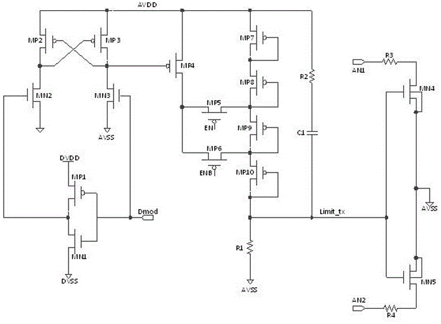
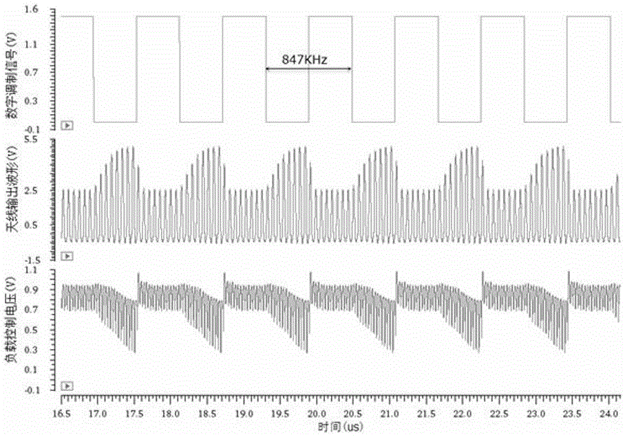
[0029] see figure 2 with image 3 , The present invention relates to a load modulation circuit compatible with NFC tags with limiting function, including a control circuit part and a main modulation circuit part connected in parallel at both ends of the antenna. The control circuit part includes: a low-voltage PMOS transisto...


PUM


Abstract

The invention relates to a load modulation circuit of an NFC tag compatible with an amplitude limiting function. The load modulation circuit comprises a control circuit part and a main modulation circuit part connected in parallel to two ends of an antenna, wherein the control circuit part comprises a low-voltage PMOS transistor MP1, a low-voltage NMOS transistor MN1, high-voltage PMOS transistors MP2, MP3, MP4, MP5, MP6, MP7, MP8, MP9 and MP10, high-voltage NMOS transistors MN2, MN3, MN4 and MN5, resistors R1, R2, R3 and R4, and a capacitor C1. The load modulation circuit has the advantages that two control functions are compatible and combined in circuit structure in circuit design, and a control signal of load modulation digital input is fused in the main modulation circuit in the control circuit, so that the design complexity and the chip area are effectively lowered.

Description

technical field [0001] The invention relates to a load modulation circuit compatible with an NFC label with a limiting function. Background technique [0002] The NFC (Near Field Communication, near field communication) tag chip is an IC chip that stores data, and it works by the electromagnetic energy sent by the NFC reading device. With the advantages of small size, light weight, low cost and long service life, it is widely used in various industries such as anti-counterfeiting and traceability of products, supply chain management, access control, and public transportation systems. [0003] The NFC tag chip is mainly composed of three core modules: RF analog front end, digital controller and memory. The RF analog front-end circuit has two input terminals, which are respectively connected to the external inductive antenna. When the NFC tag enters the alternating magnetic field of the NFC read-write device antenna, the tag antenna will obtain energy from the electromagnetic...

Claims


Application Information

Patent Timeline
IPC IPC(8): G06K19/07G06K19/077
CPCG06K19/0715G06K19/07773
Inventor 马杰易志中刘峰
Owner 中黍(北京)生物科技有限公司
Features
  • R&D
  • Intellectual Property
  • Life Sciences
  • Materials
  • Tech Scout
  • Unparalleled Data Quality
  • Higher Quality Content
  • 60% Fewer Hallucinations
Learn More