Thickening method for metalized layer of LTCC substrate
A metallized layer and substrate technology, applied in the field of microelectronics, can solve the problems of unfavorable sintering, delamination, cracking and other problems of the film layer, and achieve the effect of uniform thickness, uniform film thickness and reduction of printing times.
- Summary
- Abstract
- Description
- Claims
- Application Information
AI Technical Summary
Problems solved by technology
Method used
Image
Examples
Embodiment 1
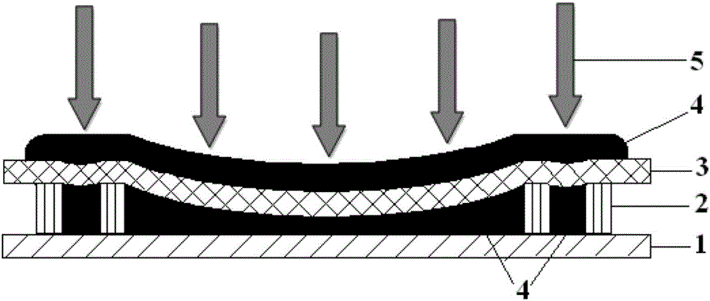
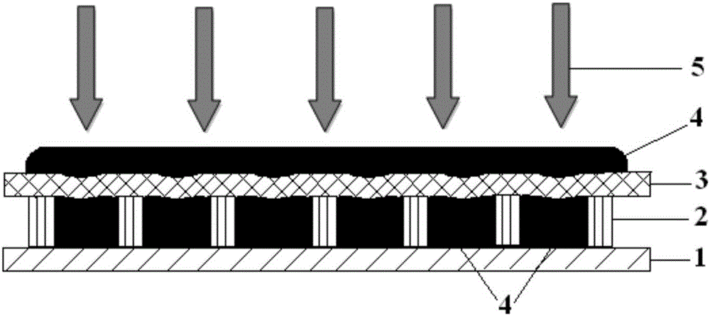
[0027] When there is no ground hole in the printed large-area conductive film layer, the surface of the LTCC substrate body 1 is preset to print the screen 3, and then the conductive paste 4 is printed to form a large-area conductive film layer, and the printed screen 3 is close to the LTCC substrate body 1. There are uniform parallel lines in the middle and around the sides on one side. The parallel lines are parallel and regularly arranged. The line width is 0.1 mm, and the line spacing is 1 mm; 23 μm, the latex thickness is 30 μm, the thickness of the middle area of the large-area conductor film layer obtained by printing once is increased by more than 60%, and the overall uniformity of the conductor is better.
Embodiment 2
[0029] When there is no ground hole in the printed large-area conductive film layer, the surface of the LTCC substrate body 1 is preset to print the screen 3, and then the conductive paste 4 is printed to form a large-area conductive film layer, and the printed screen 3 is close to the LTCC substrate body 1. There are uniform parallel lines in the middle and around the sides on one side, and the parallel lines are parallel and regularly arranged. The line width is 0.15 mm, and the line spacing is 3 mm; 23 μm, latex thickness is 30 μm, the thickness of the middle area of the large-area conductor film layer obtained by printing once is increased by more than half, the overall uniformity of the conductor is better, and the increased support latex area accounts for about 5% of the total support area.
Embodiment 3
[0031]When there is no ground hole in the printed large-area conductive film layer, the surface of the LTCC substrate body 1 is preset to print the screen 3, and then the conductive paste 4 is printed to form a large-area conductive film layer, and the printed screen 3 is close to the LTCC substrate body 1. There are uniform parallel lines in the middle and around the sides on one side. The parallel lines are parallel and regularly arranged. The line width is 0.2 mm, and the line spacing is 4 mm; 23 μm, the latex thickness is 30 μm, the thickness of the middle area of the large-area conductor film layer obtained by printing once is increased by more than one-third, and the overall uniformity of the conductor is better.
PUM
| Property | Measurement | Unit |
|---|---|---|
| Width | aaaaa | aaaaa |
| Length | aaaaa | aaaaa |
| Mesh | aaaaa | aaaaa |
Abstract
Description
Claims
Application Information
 - R&D
- Intellectual Property
- Life Sciences
- Materials
- Tech Scout
- Unparalleled Data Quality
- Higher Quality Content
- 60% Fewer Hallucinations
Browse by: Latest US Patents, China's latest patents, Technical Efficacy Thesaurus, Application Domain, Technology Topic, Popular Technical Reports.
© 2025 PatSnap. All rights reserved.Legal|Privacy policy|Modern Slavery Act Transparency Statement|Sitemap|About US| Contact US: help@patsnap.com


