Chip bonding device

A chip bonding and chip technology, which is applied in the manufacture of electrical components, electrical solid devices, semiconductor/solid devices, etc., can solve problems such as insufficient efficiency and precision, high chip failure rate, and difficulty in chip bonding, and achieve high Accuracy and high reliability, solve the difficult effect

Active Publication Date: 2017-02-01
CETC BEIJING ELECTRONICS EQUIP
View PDF11 Cites 30 Cited by
  • Summary
  • Abstract
  • Description
  • Claims
  • Application Information

AI Technical Summary

Problems solved by technology

[0006] The purpose of the present invention is to provide a chip bonding device, which detects and feeds back the position information of the chip during the chip bonding process through the visual detection feedback module, and uses the transmission module to transmit the chip to achieve high efficiency and high precision in the chip bonding process With high reliability, it solves technical problems such as difficulty in chip bonding, insufficient efficiency and precision, and high rate of bad chips in the prior art.

Method used


Image

  • Chip bonding device
  • Chip bonding device
  • Chip bonding device

Examples


Embodiment Construction

[0046] In order to make the purpose, technical solutions and advantages of the embodiments of the present invention more clear, the following will clearly and completely describe the technical solutions of the embodiments of the present invention in conjunction with the drawings of the embodiments of the present invention. Apparently, the described embodiments are some, not all, embodiments of the present invention. All other embodiments obtained by those skilled in the art based on the described embodiments of the present invention belong to the protection scope of the present invention.

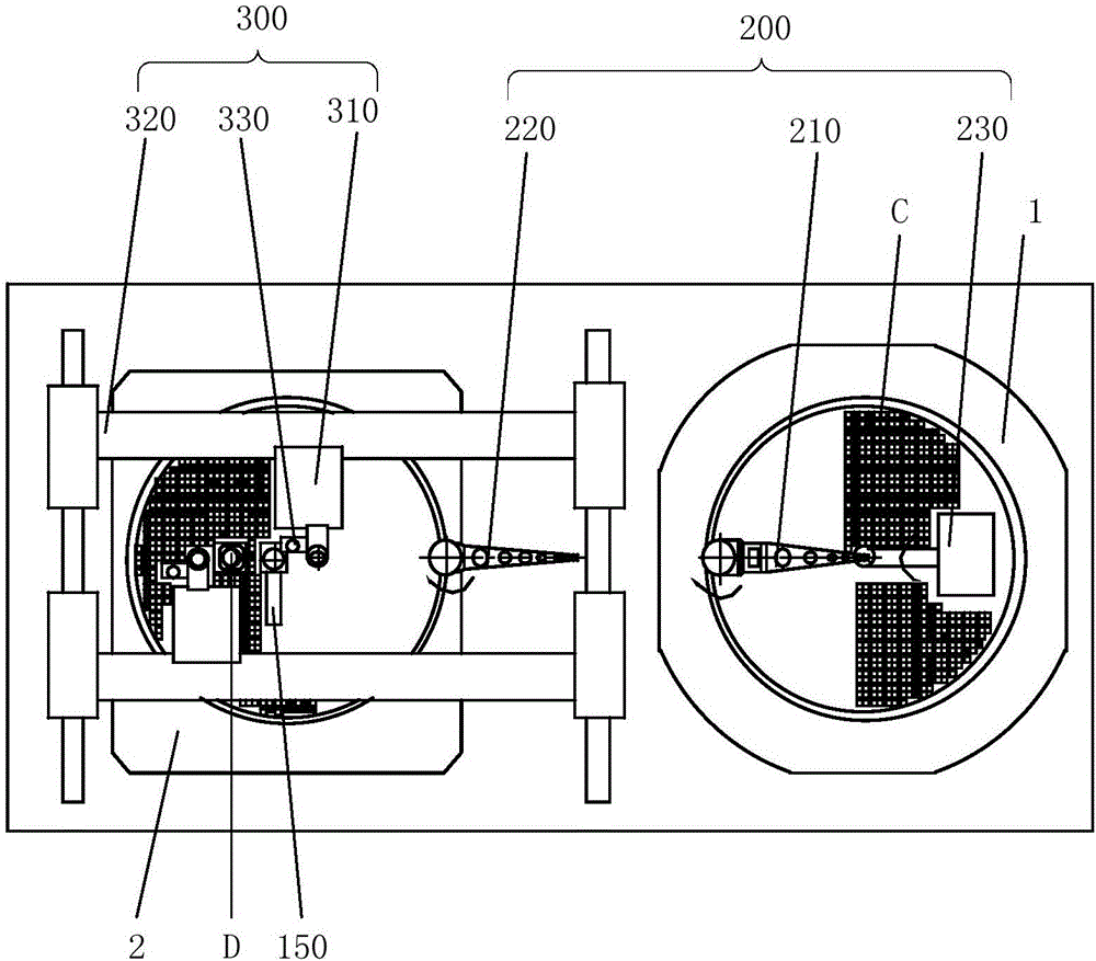
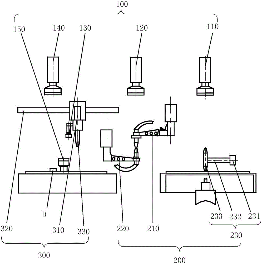
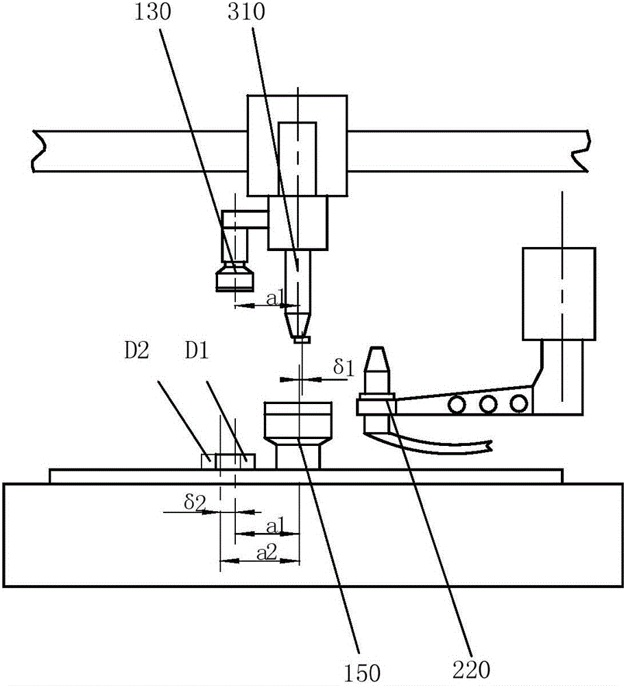
[0047] In order to solve the technical problems of chip bonding in the prior art, such as difficulty in implementing chip bonding, insufficient efficiency and precision, and a high rate of bad chips, the present invention provides a chip bonding device that uses a visual detection feedback module to monitor the position information of the chip during the chip bonding process. Detection and ...


PUM


Abstract

The invention relates to a chip bonding device comprising a first work platform, a second work platform, a visual sense detection and feedback module, a chip transmission module and a bonding module. The visual sense detection and feedback module is used for compensating position and angle deviation of chips during chip transmission processes; the chip transmission module comprises a first chip grabbing unit and a second chip grabbing unit; the first chip grabbing unit is used for picking up the chips from the first work platform according to feedback provided via a chip detection and feedback module, and the chips are conveyed to the second chip grabbing unit; the bonding module comprises a bonding head, a bonding head motion mechanism and a bonding head attracting rod; the bonding head motion mechanism and the bonding head attracting rod are used for picking up the chips from the second chip grabbing unit according to feedback provided via the visual sense detection and feedback module, then the chips are conveyed to a bonding position, and the bonding head is used for chip bonding operation. According to the chip bonding device, chip bonding efficiency and precision are improved via chip position information detection and feedback provided by the visual sense detection and feedback module.

Description

technical field [0001] The invention relates to the technical field of semiconductor device processing, in particular to a chip bonding device. Background technique [0002] With the rapid development of global electronic information technology, consumers need smaller portable electronic products, so that advanced packaging and interconnection technology is surpassing traditional technology. Advanced packaging technology integrates semiconductor packaging and assembly technology to reduce product prices, improve performance, increase density and reduce product size, making the market demand for flip-chip semiconductor packaging grow rapidly. Flip-chip packaging is an advanced chip interconnection technology, which has the characteristics of high density, high performance, thinness and shortness, and meets the development requirements of consumer electronics products such as smart phones and tablet computers. It has been obtained in PGA, BGA and CSP. It has a wide range of a...

Claims


Application Information

Patent Timeline
Patent Type & Authority Applications(China)
IPC IPC(8): H01L21/67H01L21/60
CPCH01L21/67144H01L24/80
Inventor 叶乐志霍杰王军帅周启舟郎平徐品烈成冰峰姚立新
Owner CETC BEIJING ELECTRONICS EQUIP
Why Eureka
Try Eureka