Printed circuit board and fabrication method thereof

A manufacturing method and circuit board technology, applied in the directions of printed circuits, printed circuits, printed circuit components, etc., can solve the problems of easy occurrence of voids, hidden functional dangers of circuit boards, and increased costs.

Inactive Publication Date: 2017-02-01
广东达进电子科技有限公司
View PDF10 Cites 4 Cited by
  • Summary
  • Abstract
  • Description
  • Claims
  • Application Information

AI Technical Summary

Problems solved by technology

[0005] First, the resin filled in the hole is fluid or powdery. When the resin is not cured, the resin cannot be bonded to the hole wall of the metal substrate, and the metal substrate filled with the resin needs to be subjected to high temperature for the resin. Curing treatment, however, because the resin used for filling is fluid or liquid, the adhesion of the resin before high temperature curing is not enough to leave a large volume of resin in the hole, so that the resin is easy to flow out of the hole during transportation before high temperature curing treatment Fall out of the middle, which leads to the need for an additional process to solve the problem, increasing the cost
[0006] Second, fluid resins tend to generate air bubbles during filling, and due to the high viscosity of fluid resins, it is difficult to eliminate the air bubbles, while powdery resins tend to have some spaces that cannot be filled when filling Therefore, no matter whether it is a fluid resin or a powder resin, after curing, there will be a void between the hole wall of the hole drilled on the original metal substrate and the filled resin and the center of the cured resin, which will affect the use of the circuit board. Reliability, there are functional hidden dangers
[0007] Third, when the resin-filled circuit board is subjected to alternating high and low temperature tests, the cured resin has a high probability of cracking the conductive metal layer due to the presence of air bubbles, which makes the circuit board in an alternating high and low temperature environment. There are functional hidden dangers in the system, and functional accidents are prone to occur

Method used


Image

  • Printed circuit board and fabrication method thereof
  • Printed circuit board and fabrication method thereof
  • Printed circuit board and fabrication method thereof

Examples


Embodiment Construction

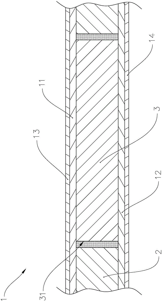
[0038] Example of a circuit board:

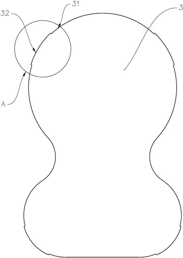
[0039] refer to figure 1 , figure 1 It is a cross-sectional schematic diagram of a circuit board semi-finished product in an embodiment of a circuit board manufacturing method of the present invention. The circuit board 1 includes a metal substrate 2, an insulating layer 11 disposed above the metal substrate 2, an insulating layer 12 disposed below the metal substrate 2, a copper foil layer 13 disposed above the insulating layer 11, and a copper foil layer disposed below the insulating layer 12. Foil layer 14. An insulating block 3 is placed in the through hole of the metal substrate 2 .

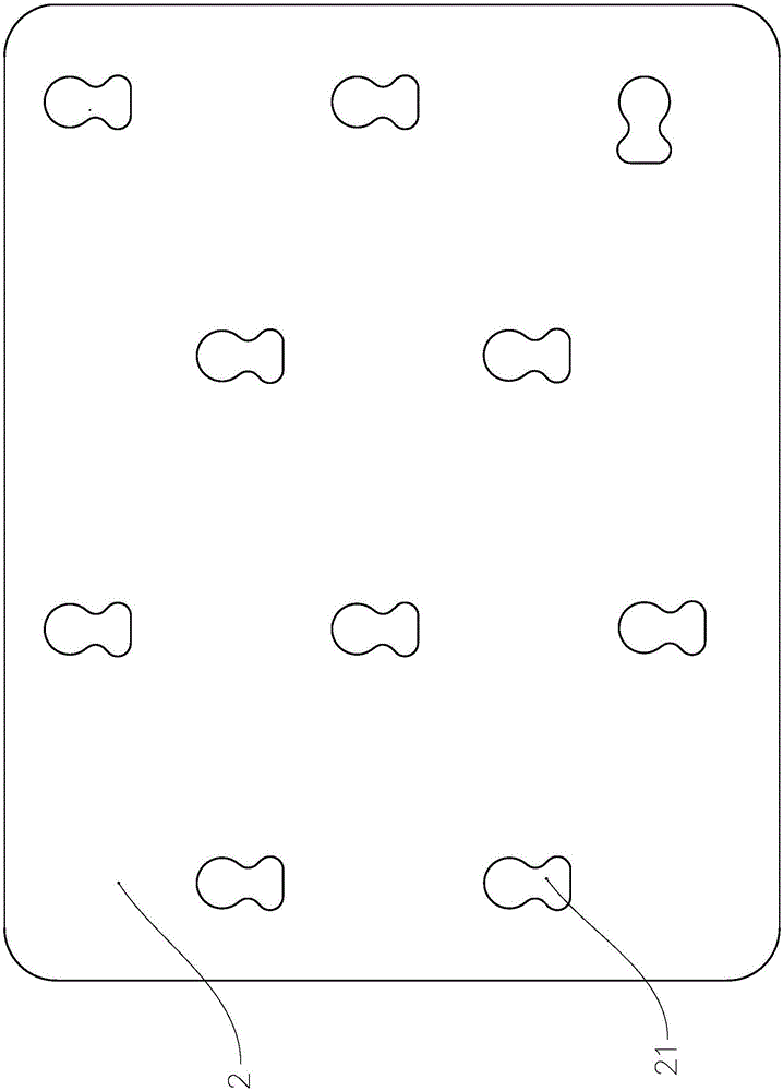
[0040] refer to figure 2 , figure 2 It is a structural schematic diagram of a metal substrate in an embodiment of a method for manufacturing a circuit board of the present invention. combine figure 1 , the metal substrate 2 can be made of copper, aluminum or other metal substrates, and one or more through holes 21 are arranged on the metal substr...


PUM


Abstract

The invention provides a printed circuit board and a fabrication method thereof. The printed circuit board comprises a metal substrate, wherein at least one through hole is formed in the metal substrate, a first insulation layer is arranged on the metal substrate, a first copper foil layer is arranged on the first insulation layer, a circuit pattern is formed on the first copper foil layer, a circle of insulation ring is arranged on an inner wall of the through hole and is formed by stamping an insulation block filled in the through hole, and the insulation block is pasted on the metal substrate by the first insulation layer when the metal substrate, the first insulation layer and the first copper foil layer are laminated. The invention also provides the fabrication method of the printed circuit board. The printed circuit board has the advantages of good working reliability and is convenient to fabricate, the fabrication method of the printed circuit board has the advantages of simple process, processing convenience, and the finished product of the printed circuit board has good working reliability.

Description

technical field [0001] The invention relates to the technical field of circuit boards, in particular to a circuit board and a method for manufacturing the circuit board. Background technique [0002] At present, the substrates used in the production of PCB boards include paper substrates, glass fiber cloth substrates, composite substrates (CEM series), laminated multilayer substrates and special material substrates (ceramic substrates, metal substrates and thermoplastic substrates) base material, etc.), and the metal base material in the special material base includes copper, aluminum, iron or other metal base materials. Generally, when a metal substrate is used as the substrate of a PCB board, holes of different shapes and sizes need to be drilled on the metal substrate, and the holes should be insulated so that the bolts or holes connecting multiple PCB boards Components passing through the hole can be kept insulated from the metal substrate. If there are circuit pattern...

Claims


Application Information

Patent Timeline
Patent Type & Authority Applications(China)
IPC IPC(8): H05K1/11
CPCH05K1/115H05K2201/0959
Inventor 黄永财
Owner 广东达进电子科技有限公司
Why Eureka
Try Eureka