Broadband wave-absorbing material and preparation method thereof

A wave-absorbing material and high-frequency wave-absorbing technology, which is applied in the field of broadband wave-absorbing materials and their preparation, can solve problems such as single product structure, poor designability, and insufficient manufacturing technology, and achieve low preparation costs, high molding efficiency, and good quality. Designable Effects

Active Publication Date: 2017-02-08
SHANGHAI RADIO EQUIP RES INST
View PDF10 Cites 38 Cited by
  • Summary
  • Abstract
  • Description
  • Claims
  • Application Information

AI Technical Summary

Problems solved by technology

With the improvement of people's awareness of the hazards of electromagnetic radiation, a series of products have appeared for civil microwave-absorbing materials, such as mobile phone radiation-proof patches, microwave-absorbing pyramids, etc., but due to the lack of manufacturing technology, the product structure is relatively simple and the designability is poor.

Method used


Image

  • Broadband wave-absorbing material and preparation method thereof
  • Broadband wave-absorbing material and preparation method thereof
  • Broadband wave-absorbing material and preparation method thereof

Examples


Embodiment

[0057] The preparation method of the low-scattering covering for field testing provided by the invention has the following steps:

[0058] 1. Design of broadband absorbing material

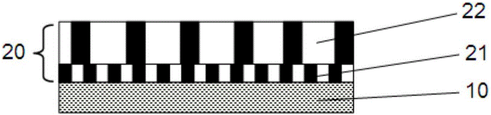
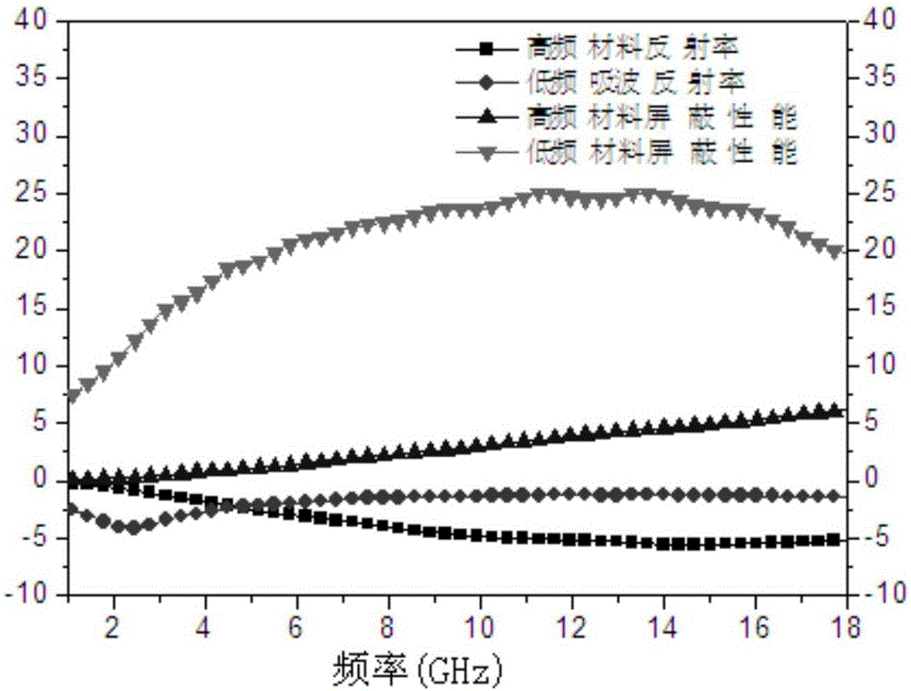
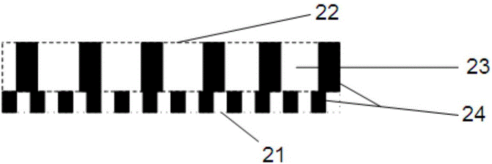
[0059] ① The absorbing materials in the high frequency range of 2-18GHz are mainly sheet-like carbonyl iron particles, and the absorbing materials in the low-frequency range of 1-2GHz are mainly sheet-type FeSi materials. The average particle size of carbonyl iron particles is generally 3-5μm. The flake FeSi particle size is close to 40-100 μm. The double-layer structure design is carried out according to the particles of two sizes, that is, the layered design of the two particle materials, the upper layer of carbonyl iron small particle absorbing material, and the lower layer of FeSi large particle absorbing material.

[0060] ②Using the multi-layer design principle to design the high-frequency wave-absorbing layer, the design frequency band is 8-18GHz. Firstly, the genetic algorithm is used to ...


PUM

PropertyMeasurementUnit
particle diameteraaaaaaaaaa
thicknessaaaaaaaaaa
thicknessaaaaaaaaaa

Abstract

The invention discloses a broadband wave-absorbing material and a preparation method thereof. The broadband wave-absorbing material is composed of a low frequency wave-absorbing material bottom layer and a high frequency wave-absorbing material surface layer. The high frequency wave-absorbing material surface layer comprises a plurality of high frequency wave-absorbing layers with different concentrations. FeSi or FeSiAl particles are taken as the additive of the low frequency wave-absorbing material, and carbonyl iron particles are taken as the additive of the high frequency wave-absorbing material. A rolling method is adopted to prepare the low frequency wave-absorbing material bottom layer, and a three-dimensional moulding technology is adopted to prepare the high frequency wave-absorbing material surface layer. The multilayer lamination manufacturing method combines a multi-rolling technology and three-dimensional moulding together and has the advantages that the binding force between layers can be ensured, multiple repeated mould pressing is avoided, the thickness of each layer, the internal structure, and particle distribution can be adjusted so as to satisfy the predetermined electromagnetic property requirements; the broadband wave-absorbing performance of the wave-absorbing material and designable performance of a shielding material can be realized; the integrated manufacturing of space structure of the wave-absorbing material is achieved, and the preparation cost is low at the same time.

Description

technical field [0001] The present invention relates to the manufacture of wave-absorbing materials with complex structures, specifically, a broadband wave-absorbing material and its preparation method. The products prepared in the present invention are aimed at civilian or military electronic equipment or instruments, and can realize the absorption of broadband electromagnetic waves , Reduce electromagnetic radiation, reduce the harm of electromagnetic radiation. Background technique [0002] With the development of electromagnetic wave technology and the wide application of communication products, the problems of electromagnetic radiation, electromagnetic scattering and electromagnetic compatibility have become increasingly prominent. The application of wave-absorbing materials provides an effective way to solve this problem. Absorbing materials can usually be divided into structural absorbing materials and coated absorbing materials. Among them, coated absorbing materials...

Claims


Application Information

Patent Timeline
Patent Type & Authority Applications(China)
IPC IPC(8): C08K7/00C08K3/36C08K3/18C08L75/04C08L33/14
CPCC08K3/18C08K3/36C08K7/00C08K2201/01C08L75/04C08L33/14
Inventor 许勇刚袁黎明王晓冰梁子长
Owner SHANGHAI RADIO EQUIP RES INST
Why Eureka
Try Eureka