A kind of manufacturing method of oxide thin film transistor and oxide thin film transistor

A technology of oxide thin film and manufacturing method, which is applied in the direction of transistors, semiconductor/solid-state device manufacturing, semiconductor devices, etc., can solve the problems of ohmic contact, poor stability of thin film transistors, and affect the surface properties of oxide semiconductor layers, etc., to achieve The effect of good electrical properties

Active Publication Date: 2019-06-21
浙江巨力宝纺织科技有限公司
View PDF3 Cites 0 Cited by
  • Summary
  • Abstract
  • Description
  • Claims
  • Application Information

AI Technical Summary

Problems solved by technology

[0003] However, since the oxide semiconductor layer is mostly an amorphous semiconductor oxide, there is a problem with its ohmic contact with the source-drain (SD) metal layer, which easily leads to poor stability of the thin film transistor.
In the prior art bottom-gate barrier type oxide semiconductor thin film transistor, during the formation of the etching barrier layer, the plasma affects the surface properties of the oxide semiconductor layer, and the source and drain metals are in contact with the oxide semiconductor whose surface properties are damaged, and finally Affecting the Electrical Properties of Oxide Thin Film Transistors

Method used


Image

  • A kind of manufacturing method of oxide thin film transistor and oxide thin film transistor
  • A kind of manufacturing method of oxide thin film transistor and oxide thin film transistor
  • A kind of manufacturing method of oxide thin film transistor and oxide thin film transistor

Examples


Embodiment 1

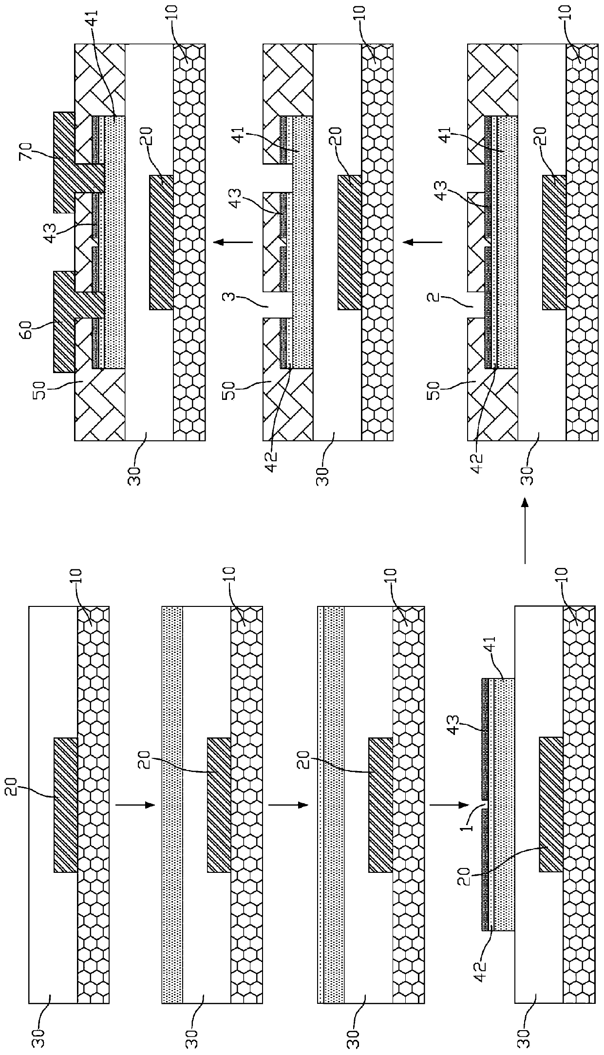
[0034] See figure 1 and figure 2 As shown, the manufacturing method of the oxide thin film transistor of this embodiment includes the following steps:

[0035] (1) sequentially forming a gate material layer and a gate insulating material layer on the substrate 10, and patterning to obtain a gate 20 and a gate insulating layer 30;

[0036] The manufacturing material of the substrate 10 includes materials such as glass, silicon wafer, quartz, plastic and silicon wafer.

[0037] The gate 20 can be formed by processes such as exposure, development, etching and sputtering, and its material can be: aluminum (Al), copper (Cu), molybdenum (Mo), titanium (Ti), silver (Ag ), gold (Au), tantalum (Ta), tungsten (W), chromium (Cr) or their alloys.

[0038] The gate insulating layer 30 can be deposited by CVD method, and its material is preferably an insulating material, including silicon dioxide, silicon nitride, silicon oxynitride or a combination of the above materials.

[0039] (2)...

Embodiment 2

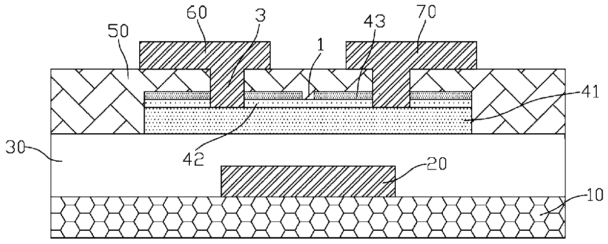
[0055] See image 3 As shown, on the basis of Embodiment 1, the method for fabricating an oxide thin film transistor in this embodiment further includes forming a fourth semi-oxide semiconductor layer between the first semi-oxide semiconductor layer 41 and the second semi-oxide semiconductor layer 42 44. The electrical conductivity of the fourth semi-oxide semiconductor layer 44 is d, where d

[0056] Yes, the material of the fourth semi-oxide semiconductor layer 44 is gallium zinc oxide, and a step is added after step (2) of Embodiment 1 to form a fourth oxide with conductivity d on the first oxide semiconductor material layer. semiconductor material layer, da, and patterned to obtain a first oxide semiconductor layer 41, a fourth oxide semiconductor layer 44, and a second oxide semiconductor layer 41. an oxide semiconductor layer 42 and a third oxide semiconductor layer 43, a first through hole 1 is formed in the third oxide semiconductor layer;

[0057] On the basis of...

Embodiment 3

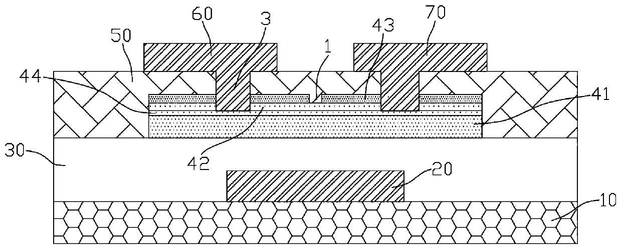
[0059] See Figure 4 As shown, on the basis of Embodiment 1, the method for fabricating an oxide thin film transistor in this embodiment further includes forming a fifth semi-oxide semiconductor layer 45 between the gate insulating layer 30 and the first semi-oxide semiconductor layer 41, and the fifth semi-oxide semiconductor layer 45 The conductivity of the oxide semiconductor layer 45 is e, where e

[0060] Yes, the material of the fifth semi-oxide semiconductor layer 45 is gallium zinc oxide, and a step is added before step (2) of Embodiment 1 to form a fifth oxide semiconductor material layer with conductivity e on the gate insulating layer 30 , ea, and pattern it to obtain the fifth oxide semiconductor layer 45, the first oxide semiconductor layer 41, the second oxide semiconductor layer 42 and the second oxide semiconductor layer. a third oxide semiconductor layer 43, a first through hole 1 is formed in the third oxide semiconductor layer;

[0061] On the basis of ...


PUM


Abstract

The invention relates to an oxide thin-film transistor manufacturing method and an oxide thin-film transistor. The manufacturing method comprises the steps of successively forming a first semi-oxide semiconductor layer, a second semi-oxide semiconductor layer and a third semi-oxide semiconductor layer in a forming process; forming a first through hole in the third semi-oxide semiconductor layer; forming an etching barrier layer on the third oxide semiconductor layer and in the first through hole; forming two through hole which penetrates through the etching barrier layer, the third oxide semiconductor layer and the second oxide semiconductor layer and are arranged at two sides of the first through hole; and forming a source electrode and a drain electrode on the etching barrier layer, wherein the source electrode and the drain electrode are connected with the first oxide semiconductor layer through the two through holes. The thin-film transistor formed according to the invention has stable and excellent electrical performance.

Description

technical field [0001] The invention relates to the technical field of semiconductor display, in particular to a method for manufacturing an oxide thin film transistor and the oxide thin film transistor. Background technique [0002] The core technology of the new flat panel display (FPD) industry is thin film transistor (TFT) backplane technology. Compared with amorphous silicon thin film transistors, the carrier concentration of oxide thin film transistors is about ten times that of amorphous silicon thin film transistors, and the carrier mobility is 20-30 times that of amorphous silicon thin film transistors. Therefore, oxide thin film transistors The charging and discharging rate of the thin film transistor to the pixel electrode can be greatly improved, the response speed of the pixel can be improved, and a faster refresh rate can be realized. Oxide thin film transistors can meet applications that require fast response and large current, such as high frequency, high re...

Claims


Application Information

Patent Timeline
Patent Type & Authority Patents(China)
IPC IPC(8): H01L29/786H01L21/336H01L29/22H01L29/10
CPCH01L29/1033H01L29/22H01L29/66969H01L29/7869
Inventor 李风浪李舒歆
Owner 浙江巨力宝纺织科技有限公司
Why Eureka
Try Eureka