AlGaInP-base light emitting diode epitaxial wafer, AlGaInP-base light emitting diode chip and preparation method thereof
A technology of light-emitting diodes and epitaxial wafers, applied in the direction of electrical components, circuits, semiconductor devices, etc., can solve problems such as poor reverse antistatic ability, reduce forward voltage, avoid excessive local current, and improve reverse antistatic effect of ability
- Summary
- Abstract
- Description
- Claims
- Application Information
AI Technical Summary
Problems solved by technology
Method used
Image

Examples
Embodiment 1
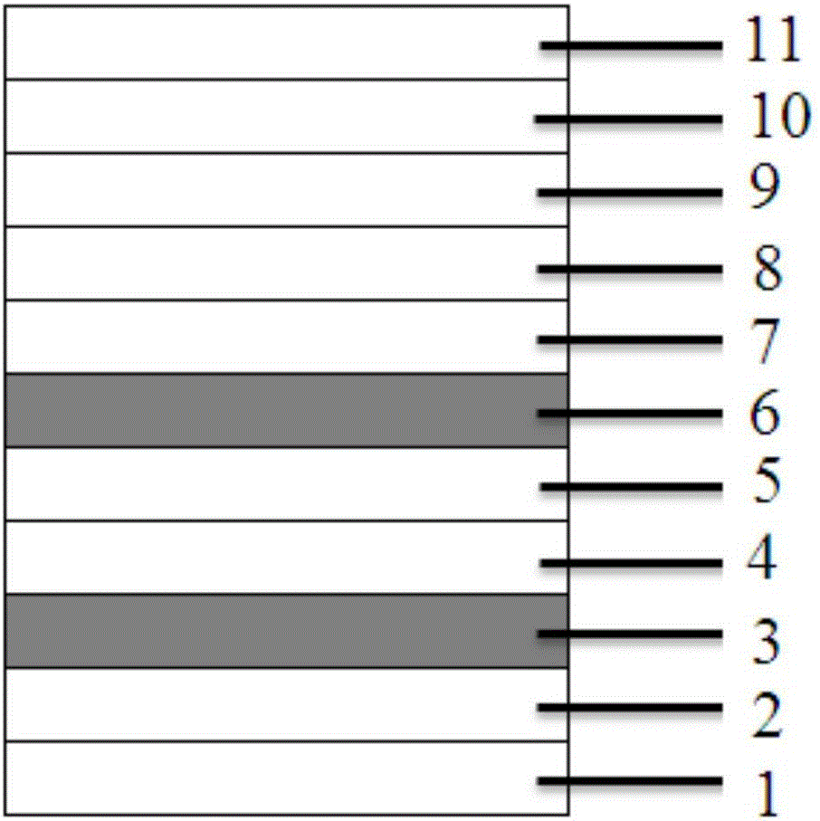
[0035] An embodiment of the present invention provides an AlGaInP-based light-emitting diode epitaxial wafer, see figure 1 , the AlGaInP-based light-emitting diode epitaxial wafer includes a GaAs substrate 1, and an N-type GaAs buffer layer 2, a dislocation barrier layer 3, an N-type GaInP etch stop layer 4, and an N+-type GaAs ohmic contact stacked on the GaAs substrate 1 in sequence. Layer 5, N+ type insertion layer 6, N type current spreading layer 7, N type confinement layer 8, active layer 9, P type confinement layer 10, P type current spreading layer 11.
[0036] It should be noted that N-type means that N-type dopant is doped, and N+ type means that the doped N-type dopant has a higher concentration than N-type, which belongs to highly doped or heavily doped.
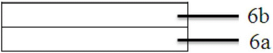
[0037] In this example, see figure 2 , the N+ type insertion layer 6 includes an N+ type GaInP layer 6a, an N+ type Al x Ga 1-x InP layer 6b, 0.3<x<0.6.
[0038]Optionally, the thickness of the N+ type GaInP...
Embodiment 2
[0056] The embodiment of the present invention provides a method for preparing an AlGaInP-based light-emitting diode epitaxial wafer, which is suitable for preparing the AlGaInP-based light-emitting diode epitaxial wafer provided in Example 1. See Figure 5 , the preparation method comprises:
[0057] Step 201: growing an N-type GaAs buffer layer on a GaAs substrate.
[0058] Optionally, the thickness of the N-type GaAs buffer layer may be 150-300 nm, the growth temperature may be 650-670° C., V / III may be 20-30, and the growth rate may be 0.5-0.8 nm / s.
[0059] Wherein, V / III is the molar concentration ratio of atoms with valence V to atoms with valence III.
[0060] Step 202: growing a dislocation blocking layer on the N-type GaAs buffer layer.
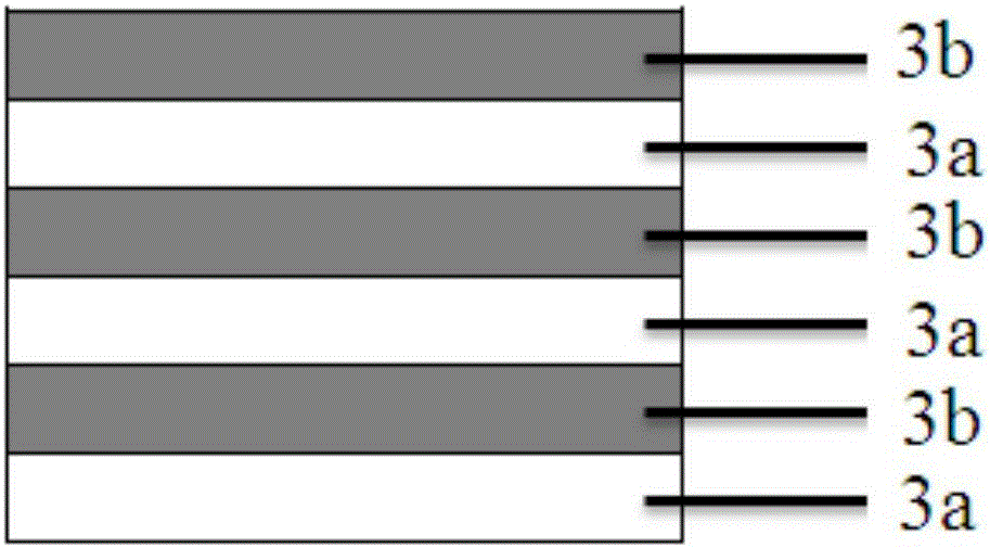
[0061] Specifically, the dislocation blocking layer includes alternately stacked first sublayers and second sublayers, the first sublayer is an AlAs layer, and the second sublayer is a GaAs layer or an Al y Ga 1-y As layer, 0.5<...
Embodiment 3
[0091] An embodiment of the present invention provides an AlGaInP-based light-emitting diode chip, see Figure 6 The AlGaInP-based light-emitting diode chip includes a substrate 12, and a P-type current spreading layer 11, a P-type confinement layer 10, an active layer 9, an N-type confinement layer 8, an N-type current spreading layer 7, N+ type insertion layer 6 and N+ type GaAs ohmic contact layer 5 .
[0092] In this embodiment, the N+ type insertion layer includes N+ type Al which is sequentially stacked on the N type current spreading layer. x Ga 1-x InP layer, N+ type GaInP layer, 0.3
[0093] Optionally, the thickness of the N+ type GaInP layer can be 10-20 nm, the doping concentration can be 3E18-6E18, and the N-type dopant can be SiH 4 、Si 2 h 6 , Te(C 2 h 5 ) 2 any of the.
[0094] Optionally, N+ type Al x Ga 1-x The thickness of the InP layer can be 10-20nm, the doping concentration can be 3E18-6E18, and the N-type dopant can be SiH 4 、Si 2 h 6...
PUM
| Property | Measurement | Unit |
|---|---|---|
| Thickness | aaaaa | aaaaa |
| Thickness | aaaaa | aaaaa |
Abstract
Description
Claims
Application Information
 - R&D
- Intellectual Property
- Life Sciences
- Materials
- Tech Scout
- Unparalleled Data Quality
- Higher Quality Content
- 60% Fewer Hallucinations
Browse by: Latest US Patents, China's latest patents, Technical Efficacy Thesaurus, Application Domain, Technology Topic, Popular Technical Reports.
© 2025 PatSnap. All rights reserved.Legal|Privacy policy|Modern Slavery Act Transparency Statement|Sitemap|About US| Contact US: help@patsnap.com