A digital chip function testing method and system

A technology for digital chip and functional testing, applied in digital circuit testing, electronic circuit testing, electrical measurement, etc., can solve the problem of low test accuracy, achieve comprehensive functional testing, and improve accuracy and reliability.

Active Publication Date: 2019-04-23
XIDIAN UNIV
View PDF6 Cites 0 Cited by
  • Summary
  • Abstract
  • Description
  • Claims
  • Application Information

AI Technical Summary

Problems solved by technology

[0005] The purpose of the present invention is to overcome the deficiencies of the above-mentioned prior art, and provide a digital chip function testing method and system for solving the technical problem of low test accuracy existing in the prior art

Method used


Image

  • A digital chip function testing method and system
  • A digital chip function testing method and system
  • A digital chip function testing method and system

Examples


Embodiment Construction

[0029] The present invention will be further specifically described below in conjunction with the accompanying drawings and embodiments.

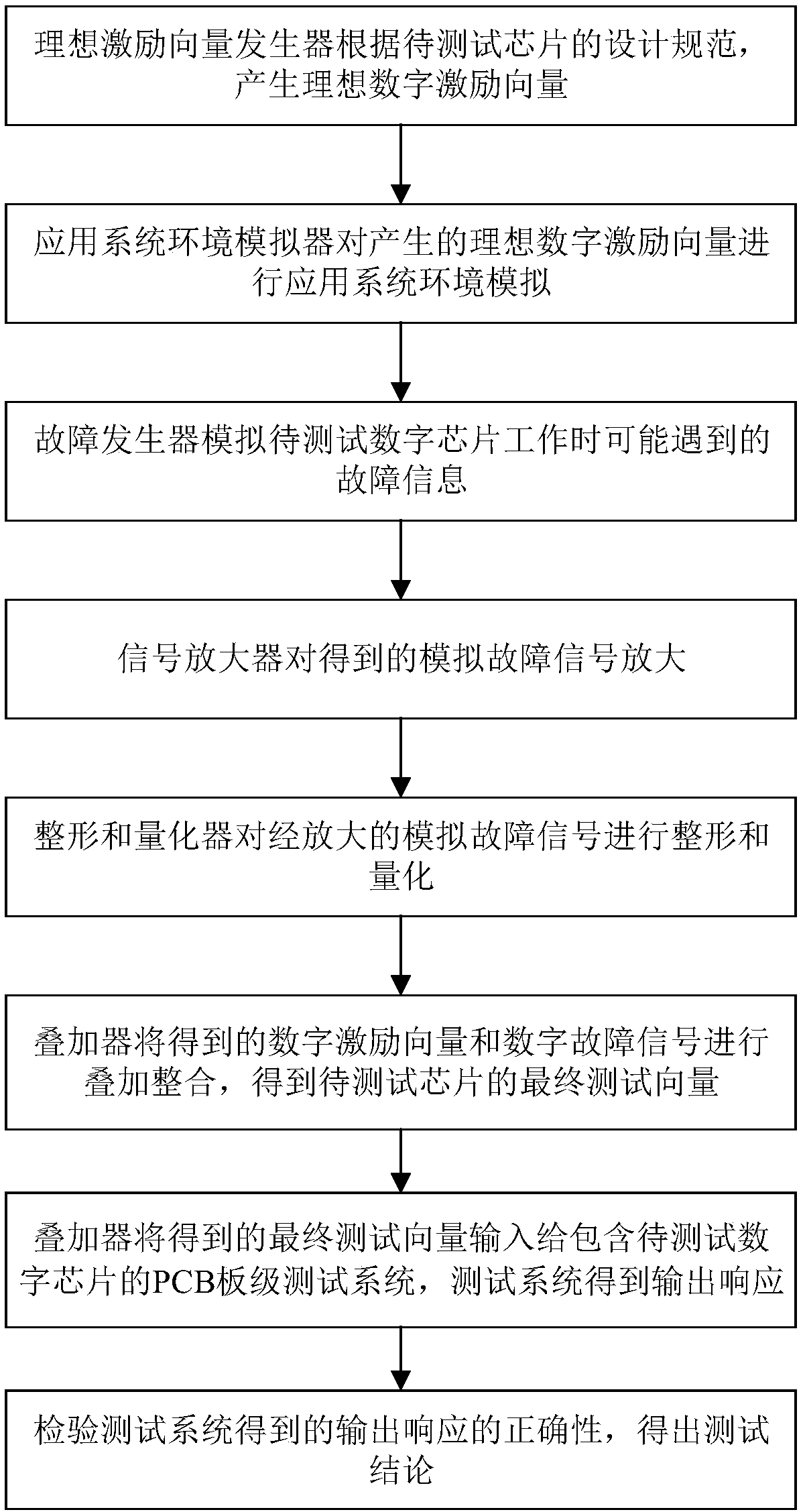
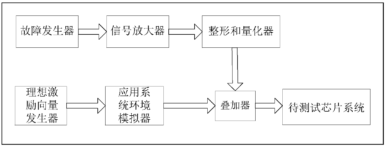
[0030] Refer to attached figure 1 , to further describe the digital chip function testing method of the present invention.

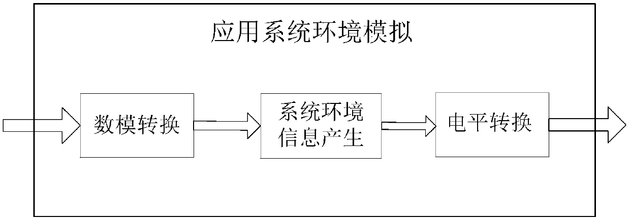
[0031] The most important thing about the digital chip function testing method of the present invention is to take into account the system environment information of the actual work of the digital chip and the influence of the fault information that the chip may encounter during operation, and simulate its real system environment and fault information by a certain method. Test the impact of the ideal stimulus received by the physical digital chip interface, integrate the system environment fault information and the signal integrity problems brought by the fault information into the basic test vector, so as to use the test vector containing the system environment fault information and fault information to To test the ...


PUM


Abstract

The invention provides a digital chip function test method and system. The objective of the invention is to solve the technical problem of low test accuracy in the prior art. According to the digital chip function test method and system of the invention, influence on test results caused by application system environment factors and fault information is considered. The test method includes the following steps that: an ideal digital excitation vector is generated; application system environment simulation is carried out; fault information simulation is carried out; simulation fault signals are amplified; shaping and quantization are carried out; the ideal digital excitation vector which has been subjected to application system environment influence, and fault information are superposed, so that a final test vector is generated; the final test vector is inputted into a chip system to be tested; and the correctness of response is detected, a test conclusion is obtained. The test system includes a fault generator, a signal amplifier, a shaping and quantization device, an ideal excitation vector generator and an application system environment simulator, wherein the fault generator, the signal amplifier and the shaping and quantization device are connected with one another sequentially, and the ideal excitation vector generator and the application system environment simulator are connected with each other; the output ends of the shaping and quantization device and the application system environment simulator are connected with an adder; and the output end of the adder is connected to the chip system to be tested.

Description

technical field [0001] The invention belongs to the field of digital chip testing, and relates to a digital chip function testing method and system considering application system environmental factors and fault information, which can be used in the technical field related to digital chips. Background technique [0002] The chip industry is a national strategic emerging industry and an important foundation for national economy and social informatization, and chip testing technology is an important part of the chip industry. Chip manufacturing is a process with fine structure, complex process, and cumbersome process. It will inevitably leave potential defects in the production process, so that the reliability level of the device cannot meet the standard requirements, and failures may occur at any time due to various reasons. During chip processing, material impurity and defects, equipment imperfections, and human errors are all causes of failures, so chip testing during the de...

Claims


Application Information

Patent Timeline
Patent Type & Authority Patents(China)
IPC IPC(8): G01R31/319G01R31/3183
CPCG01R31/318371G01R31/31917
Inventor 史江义李钊缪磊马佩军古生霖舒浩
Owner XIDIAN UNIV
Why Eureka
Try Eureka