Semiconductor device and formation method thereof

A semiconductor and device technology, applied in the field of semiconductor devices and their formation, can solve problems such as poor performance of MOS transistors

Active Publication Date: 2017-02-15
SEMICON MFG INT (SHANGHAI) CORP +1
View PDF4 Cites 8 Cited by
  • Summary
  • Abstract
  • Description
  • Claims
  • Application Information

AI Technical Summary

Problems solved by technology

[0004] However, as the feature size shrinks further, the performance of MOS transistors formed in the prior art is poor

Method used


Image

  • Semiconductor device and formation method thereof
  • Semiconductor device and formation method thereof
  • Semiconductor device and formation method thereof

Examples


Embodiment Construction

[0035] As the feature size is further reduced, the performance of semiconductor devices formed in the prior art is poor.

[0036] Figure 1 to Figure 3 It is a structural schematic diagram of the formation process of a semiconductor device in an embodiment of the present invention.

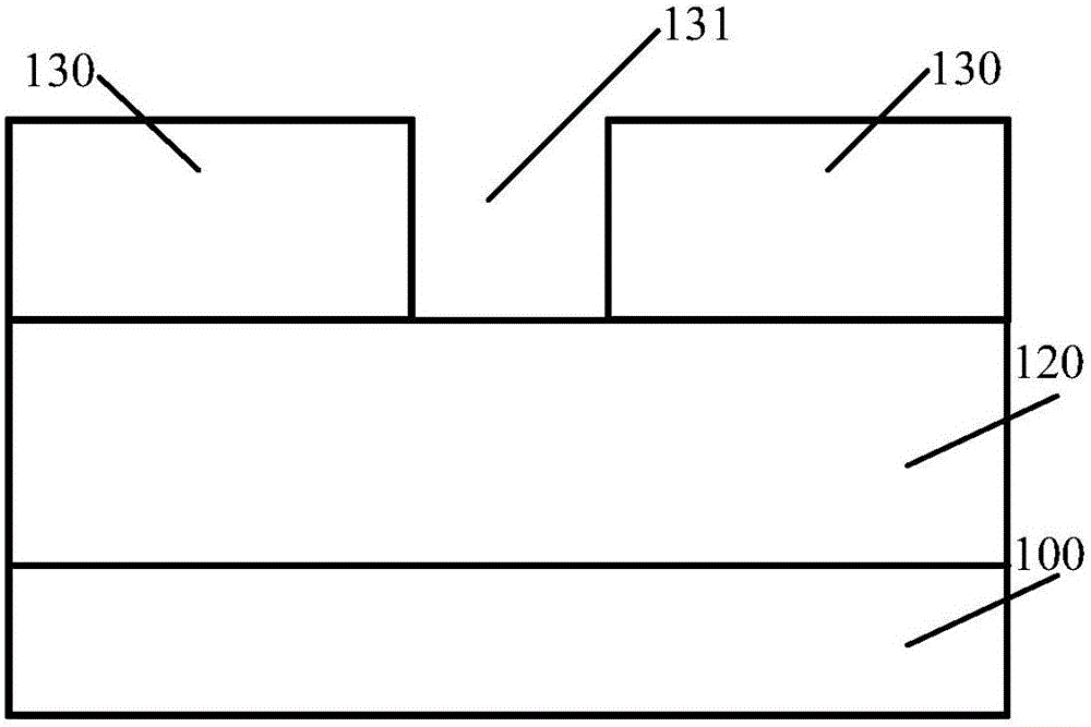
[0037] refer to figure 1 , providing a base, the base includes a substrate 100 and a fin 120 located on the surface of the substrate 100; an interlayer dielectric layer 130 is formed on the surface of the base, and a groove 131 is formed in the interlayer dielectric layer 130, so The groove 131 exposes the top surface and the sidewall of the fin 120 .

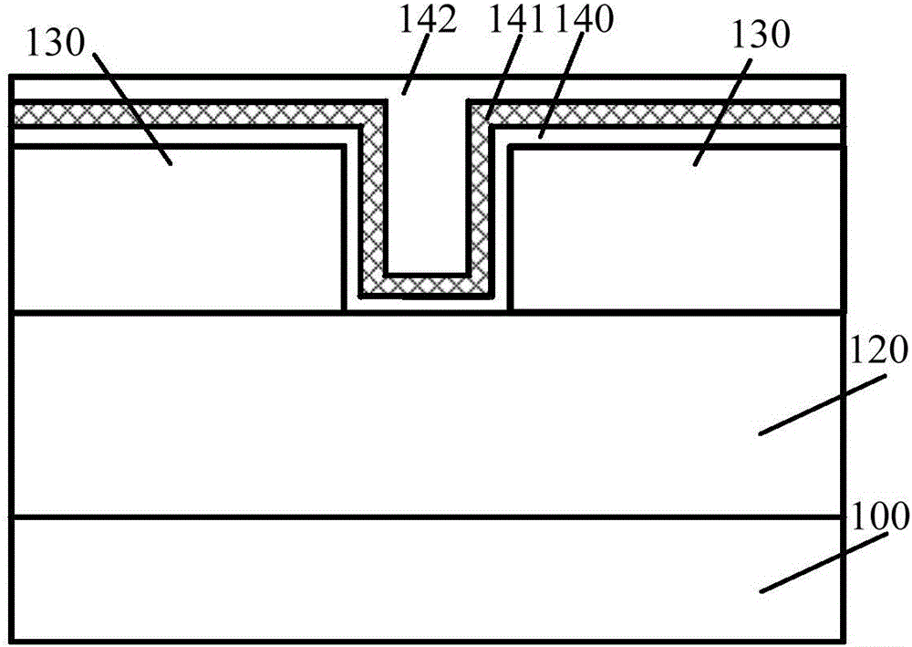
[0038] refer to figure 2 , formed to cover the groove 131 (refer to figure 1 ) a gate dielectric layer 140 at the bottom and sidewalls; forming a barrier layer 141 covering the gate dielectric layer 140; forming a metal layer 142 covering the barrier layer 141, the entire surface of the metal layer 142 being higher than the interlayer dielect...


PUM

PropertyMeasurementUnit
Thicknessaaaaaaaaaa
Thicknessaaaaaaaaaa

Abstract

The invention provides a semiconductor device and a formation method thereof. The formation method of the semiconductor device comprises steps: providing a substrate, wherein the surface of the substrate is provided with an interlayer dielectric layer, a groove is arranged in the interlayer dielectric layer, and the surface of the substrate is exposed by the groove; forming a gate dielectric layer which covers the bottom and sidewalls of the groove; forming a first barrier layer which covers the gate dielectric layer; performing non-crystallization processing on the first barrier layer to convert the first barrier layer to a second barrier layer; and forming a metal layer which covers the second barrier layer, wherein the surface of the metal layer is aligned with the surface of the interlayer dielectric layer. According to the semiconductor device and the formation method thereof, the performance of the semiconductor device is improved.

Description

technical field [0001] The invention relates to the field of semiconductor manufacturing, in particular to a semiconductor device and a forming method thereof. Background technique [0002] MOS transistors are one of the most important components in modern integrated circuits. The basic structure of a MOS transistor includes: a semiconductor substrate; a gate structure located on the surface of the substrate, a source region located in the semiconductor substrate on one side of the gate structure, and a drain region located in the semiconductor substrate on the other side of the gate structure. The MOS transistor generates a switching signal by applying a voltage to the gate structure and adjusting the current through the channel at the bottom of the gate structure. [0003] With the increasing integration of MOS transistors, the voltage and current required for the operation of MOS transistors continue to decrease, and the switching speed of transistors increases according...

Claims


Application Information

Patent Timeline
IPC IPC(8): H01L21/336H01L29/78
CPCH01L29/66545H01L29/66795H01L29/78H01L29/785
Inventor 周飞
Owner SEMICON MFG INT (SHANGHAI) CORP
Why Eureka
Try Eureka