Non-contact wafer annealing device and method

A non-contact, annealing device technology, applied in electrical components, semiconductor/solid-state device manufacturing, circuits, etc., can solve the problems affecting the electrical properties of semiconductor chips, uneven wafer heating temperature, uneven wafer annealing temperature, etc. Achieve highly automated flow operation, uniform wafer annealing temperature, and realize the effect of flow operation

Pending Publication Date: 2017-02-15
珠海鼎泰芯源晶体有限公司
View PDF4 Cites 7 Cited by
  • Summary
  • Abstract
  • Description
  • Claims
  • Application Information

AI Technical Summary

Problems solved by technology

Thermocouples are usually used to measure the temperature of the backlight surface. The contact measurement of thermocouples is obviously limited, which may cause damage to the wafer surface, and the measurement accuracy is average.
The contact between the quartz frame and the wafer will affect the heat transfer on the surface of the wafer; due to the difference in the irradiation of different lamp tubes, if the irradiation of the lamp tube is controlled centrally, this will cause uneven annealing temperature of the wafer
In some processes, integrated circuits have been produced on the front of the wafer, and the back of the wafer needs to be annealed, so the front of the wafer is not suitable for contact with quartz. If it does, it will easily cause damage to the integrated circuits on the front and the heating temperature of the wafer Inhomogeneity; if only the bracket is used to support the edge of the wafer and the backside is heated and annealed, the wafer will be deformed due to thermal stress during the annealing process, especially for large-sized wafers
[0004] Uneven annealing temperature and wafer surface damage will directly affect the electrical properties of semiconductor chips. Therefore, how to avoid the above problems is an urgent problem to be solved in related fields.

Method used


Image

  • Non-contact wafer annealing device and method
  • Non-contact wafer annealing device and method

Examples


Embodiment Construction

[0025] The following will clearly and completely describe the technical solutions in the embodiments of the present invention in conjunction with the accompanying drawings in the embodiments of the present invention:

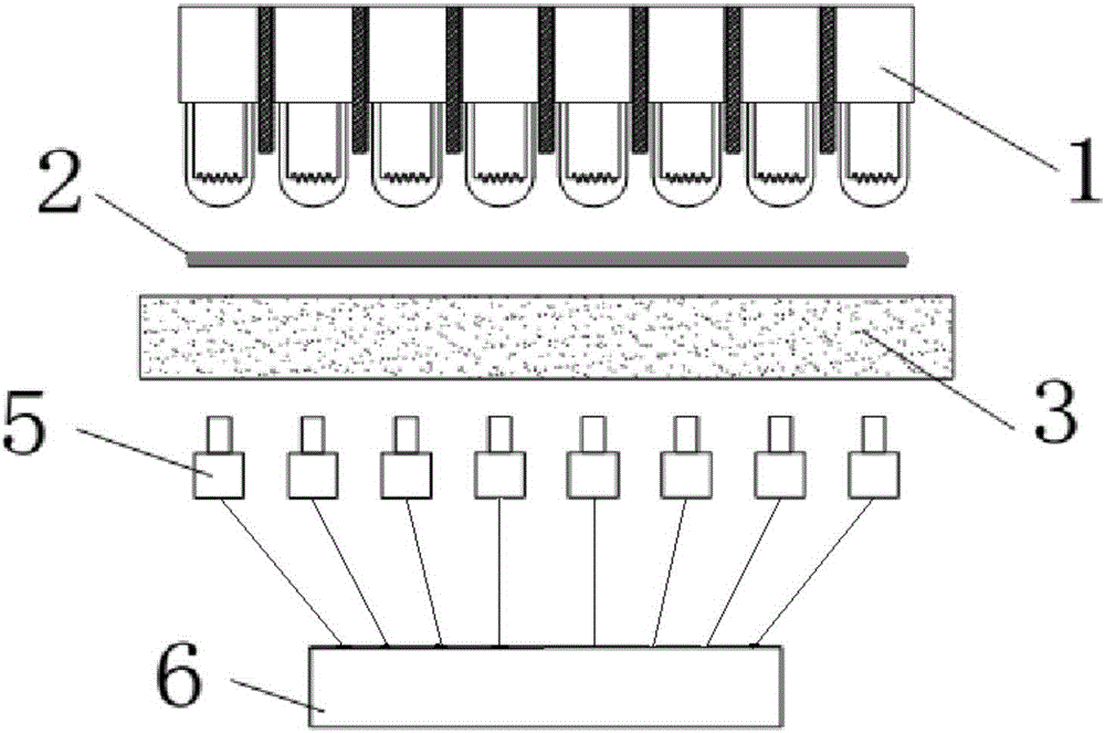
[0026] like figure 1 , 2 As shown, a non-contact wafer annealing device includes a wafer 2, an air bearing platform 3, a light source, an infrared temperature measuring probe 5, and a controller 6, wherein:

[0027] The light source is arranged in an array of lamp tubes 1, and different lamp tubes 1 illuminate different positions on the surface of the wafer 2;

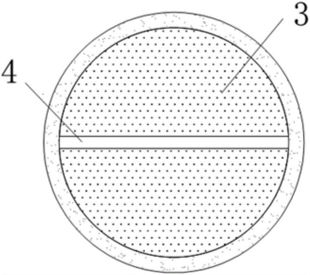
[0028] The cross-section of the air-floating stage 3 is circular, and a temperature measuring hole 4 is arranged in the middle, the temperature measuring hole 4 is located at the diameter of the air-floating stage 3, and the length of the temperature measuring hole 4 is greater than or equal to the diameter of the wafer 2 length. The width of the temperature measurement hole 4 is determined according ...


PUM


Abstract

The present invention discloses a non-contact wafer annealing device and method. The device comprises a wafer, an air floating platform deck, a light source, an infrared temperature measurement probe and a controller. A plurality of air holes are uniformly distributed on the air floating platform deck, air is pumped in from the air holes to form an air cushion for supporting the wafer; the light source is arranged right above the wafer, and the wafer is heated through radiation; the infrared temperature measurement probe is arranged at the right below the air floating platform deck, and the temperature of the wafer is measured through the temperature measurement hole arranged at the diameter of the air floating platform deck; and the controller is connected with the infrared temperature measurement probe. The non-contact wafer annealing device and method are simple to perform, the annealing temperature is uniform, the measurement precision is high, and the non-contact wafer annealing device and method can avoid damaging the wafer and perform annealing of the back surface of the wafer while the fashioned front surface and the edges of the wafer do not damaged and can realize the automation operation.

Description

technical field [0001] The invention relates to a wafer annealing device and an annealing method thereof, in particular to a non-contact wafer annealing device and an annealing method thereof. Background technique [0002] With the advancement of technology, semiconductor chips have been applied to various fields of social life, and chips are usually made of wafers, such as silicon or other semiconductor material wafers. In the manufacturing process, according to different processes, such as alloying, oxidation or nitriding, ion implantation annealing, doping activation, and gettering, etc., it is often necessary to perform multi-step annealing heat treatment on the wafer to repair the damage of the crystal and eliminate Dislocations and native defects. [0003] In the prior art, the wafer is usually placed on a quartz rack in the process chamber, and the wafer is heated by high-intensity light source radiation. The light source is usually a lamp tube arranged in an array,...

Claims


Application Information

Patent Timeline
Patent Type & Authority Applications(China)
IPC IPC(8): H01L21/67
CPCH01L21/67115H01L21/67248
Inventor 杨翠柏杨光辉陈丙振方聪
Owner 珠海鼎泰芯源晶体有限公司
Why Eureka
Try Eureka