Display panel, display panel motherboard and manufacturing method thereof

A display panel and manufacturing method technology, applied in the direction of final product manufacturing, sustainable manufacturing/processing, semiconductor/solid-state device manufacturing, etc., can solve problems such as shortened life, abnormal display, and enlarged frame area, so as to ensure heat conduction and improve cutting Yield rate, damage reduction effect

Inactive Publication Date: 2017-02-15
SHANGHAI TIANMA MICRO ELECTRONICS CO LTD +1
View PDF6 Cites 20 Cited by
  • Summary
  • Abstract
  • Description
  • Claims
  • Application Information

AI Technical Summary

Problems solved by technology

Due to the large amount of heat generated during the laser cutting process, the heat will diffuse to the functional film layers related to the display and damage the functional layers, such as the electrical characteristics of the thin film transistor and the sealing effect of the thin film packaging layer, making the The functional layer is vulnerable to water and oxygen corrosion, resulting in abnormal display and shortened lifespan
Although the above problems can be solved by keeping the cutting area away from the functional layer related to the display, it will also bring about the problem of expanding the frame area, which does not conform to the development trend of narrow frame design

Method used


Image

  • Display panel, display panel motherboard and manufacturing method thereof
  • Display panel, display panel motherboard and manufacturing method thereof
  • Display panel, display panel motherboard and manufacturing method thereof

Examples


Embodiment Construction

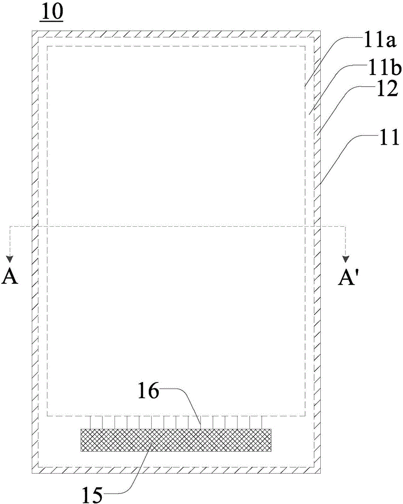
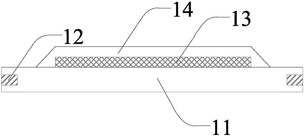
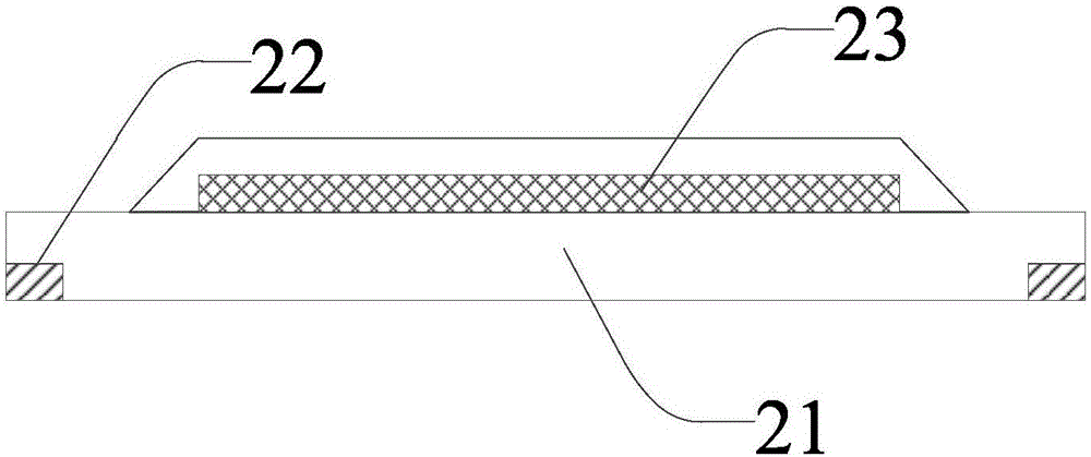
[0024] Example embodiments will now be described more fully with reference to the accompanying drawings. Example embodiments may, however, be embodied in many forms and should not be construed as limited to the embodiments set forth herein; rather, these embodiments are provided so that this disclosure will be thorough and complete, and will fully convey the concept of example embodiments to those skilled in the art. The same reference numerals denote the same or similar structures in the drawings, and thus their repeated descriptions will be omitted.

[0025] The words expressing position and direction described in the present invention are all described by taking the accompanying drawings as an example, but changes can also be made according to needs, and all changes are included in the protection scope of the present invention. The accompanying drawings of the present invention are only used to illustrate the relative positional relationship, and the layer thickness of som...


PUM


Abstract

The invention provides a display panel, a display panel motherboard and a manufacturing method thereof. The display panel comprises a substrate comprising a display region and a frame region surrounding the display region; a display element arranged on the substrate and in the display region; and a heat-conductive pattern layer arranged in the frame region of the substrate, wherein at least a part of the heat-conductive pattern layer is embedded in the substrate, and the heat-conductive pattern layer surrounds the display region. In the cutting process of the display panel motherboard, the generated heat can be absorbed or exported by the heat-conductive pattern layer, so that damage to the display element and a film encapsulation layer can be reduced; and meanwhile, reduction of heat conduction and heat absorption performance due to melt and breakage of the heat-conductive pattern layer can be prevented, and thus heat conduction and heat absorption effects of the heat-conductive pattern layer are ensured, and cutting qualified rate is improved.

Description

technical field [0001] The invention relates to the field of display technology, in particular to a display panel, a display panel motherboard and a manufacturing method thereof. Background technique [0002] With the continuous development of display technology, the display panel manufacturing technology is becoming more and more mature. Existing display panels mainly include Organic Light Emitting Diode (OLED), Liquid Crystal Display (LCD), A plasma display panel (Plasma Display Panel, PDP) and the like. The flexible display panel is a deformable and bendable display device made of materials such as polyimide or polyester film. Compared with the traditional display panel, the flexible display panel has the advantages of small size, low power consumption, With the advantages of being bendable and flexible, it is a display panel with broad application prospects. [0003] The manufacturing process of the existing flexible display panel is usually as follows: a flexible subs...

Claims


Application Information

Patent Timeline
Patent Type & Authority Applications(China)
IPC IPC(8): H01L27/32H01L51/00H01L51/52H01L51/56
CPCH10K59/12H10K71/80H10K77/111H10K50/87H10K71/00Y02E10/549Y02P70/50
Inventor 翟应腾
Owner SHANGHAI TIANMA MICRO ELECTRONICS CO LTD
Why Eureka
Try Eureka