Thin-film transistor structure

A thin film transistor and semiconductor technology, applied in transistors, semiconductor devices, electrical components, etc., can solve problems such as limiting the current conductivity of components, low carrier mobility, and high resistivity of amorphous silicon semiconductor layers.

Inactive Publication Date: 2017-02-15
GIANTPLUS TECH
View PDF5 Cites 7 Cited by
  • Summary
  • Abstract
  • Description
  • Claims
  • Application Information

AI Technical Summary

Problems solved by technology

In thin film transistors, according to the different semiconductor layer materials, it can be subdivided into polysilicon thin film transistors and amorphous silicon thin film transistors. Polysilicon thin film transistors have the advantage of high carrier mobility, but at the same time they have a large leakage current. The disadvantage of amorphous silicon thin film transistors is that the carrier mobility of amorphous silicon thin film transistors is lower than that of polycrystalline silicon thin film transistors. This factor causes the amorphous silicon semiconductor layer to have a higher resistivity, which in turn limits the conductivity of the component current. The turn-on current of the transistor will also indirectly cause the driving efficiency to be less than ideal

Method used


Image

  • Thin-film transistor structure
  • Thin-film transistor structure
  • Thin-film transistor structure

Examples


Embodiment Construction

[0025] In order to enable the examiner to have a further understanding and understanding of the features and achieved effects of the present invention, the following examples and accompanying drawings are attached herewith:

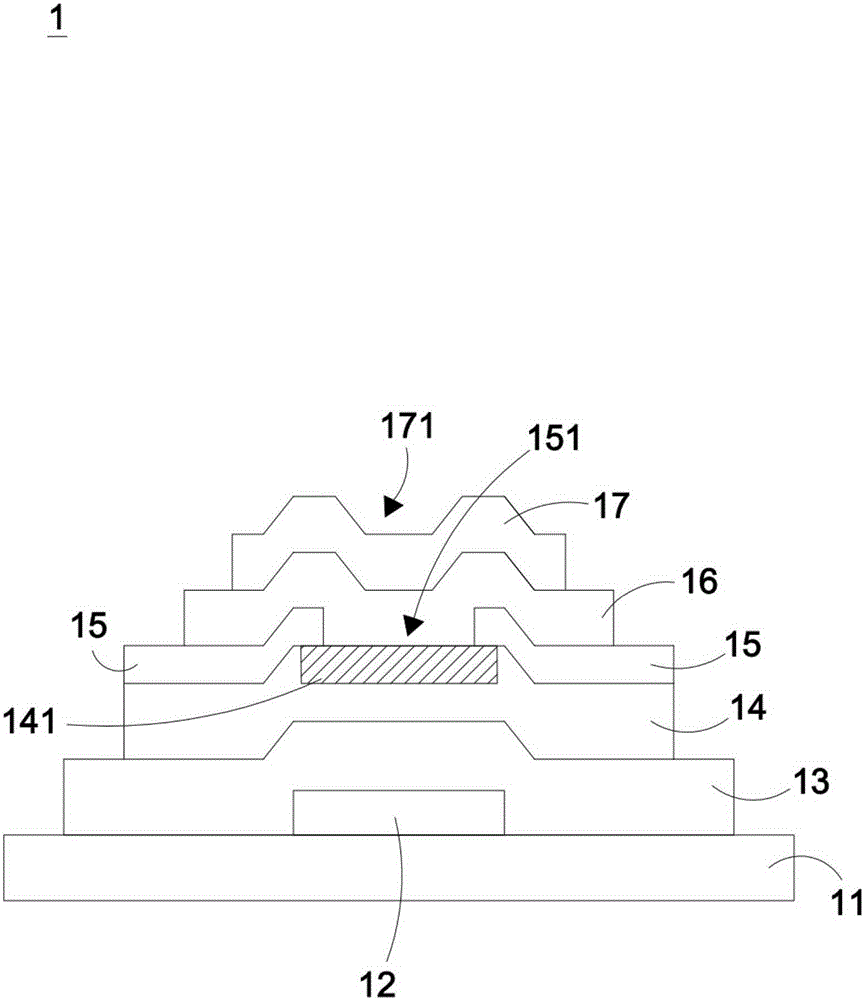
[0026] One of the characteristics of the present invention is that: in view of the increasing demand for the driving performance of the transistor and the miniaturization of the circuit layout by the structure of the thin film transistor, the present invention proposes a thin film transistor structure to increase the on-current to improve the driving performance and optimize circuit layout area, etc.

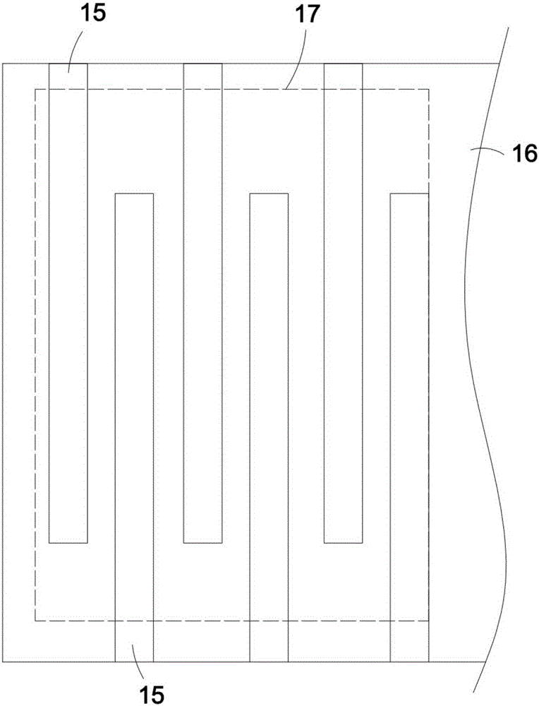
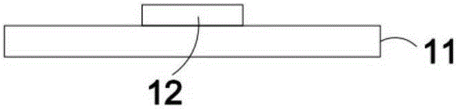
[0027] Such as Figure 1A Shown is a schematic structural diagram of the first embodiment of the present invention. As shown in the figure, it illustrates the components of this embodiment and their connection relationship. This embodiment is a thin film transistor structure 1, which includes a substrate 11, a first metal layer 12, a first buffer layer 13, ...


PUM


Abstract

The present invention provides a thin-film transistor structure, which comprises a substrate, a first metal layer, a first buffer layer, a semiconductor layer, a second metal layer, a second buffer layer, and a third metal layer. The second metal layer includes a gap region; the semiconductor layer includes a channel region. The present invention uses the first and third metal layers to form double gates. By controlling the channel region using the double-gate structure, the turn-on current of the thin-film transistor can be enhanced and thus achieving the efficacy of improving the driving efficiency of the device.

Description

technical field [0001] The invention relates to a thin film transistor structure, especially a thin film transistor structure with double gates. Background technique [0002] In the flat panel display industry, Thin Film Transistor Liquid Crystal Display (TFTL-LCD) is the hottest product today, and because thin film transistors are widely used in flat panel display products, the quality of thin film transistors (such as current conduction, etc.) The overall quality of the display has an inseparable relationship. [0003] When the TFT is turned on, electrons will diffuse from the source to the drain. In thin film transistors, according to the different semiconductor layer materials, it can be subdivided into polysilicon thin film transistors and amorphous silicon thin film transistors. Polysilicon thin film transistors have the advantage of high carrier mobility, but at the same time they have a large leakage current. The disadvantage of amorphous silicon thin film transist...

Claims


Application Information

Patent Timeline
Patent Type & Authority Applications(China)
IPC IPC(8): H01L29/786H01L29/423
CPCH01L29/42384H01L29/78648H01L29/4908H01L29/78663H01L29/78672H01L29/78696
Inventor 周凯茹吴哲耀赖谷皇江宜达
Owner GIANTPLUS TECH
Why Eureka
Try Eureka