Optimized analog signal conditioning circuit and working method thereof

An analog signal and circuit conditioning technology, applied in electrical components, analog-to-digital converters, analog-to-digital conversion, etc., can solve the problems of long signal transmission distance, complex circuit structure, increased time cost, etc., to avoid repeated design and optimization. Circuit structure, the effect of saving time and cost

Pending Publication Date: 2017-02-15
ELECTRIC POWER RES INST OF STATE GRID ANHUI ELECTRIC POWER +1
View PDF4 Cites 5 Cited by
  • Summary
  • Abstract
  • Description
  • Claims
  • Application Information

AI Technical Summary

Problems solved by technology

[0004] The present invention provides an optimized analog signal conditioning circuit in order to solve the problems of the existing analog signal conditioning circuit that many devices are used, the circuit structure is complex, the signal transmission distance is long, the occupied area is large, the failu

Method used


Image

  • Optimized analog signal conditioning circuit and working method thereof
  • Optimized analog signal conditioning circuit and working method thereof
  • Optimized analog signal conditioning circuit and working method thereof

Examples


Embodiment Construction

[0029] In order to make the technical means, creative features, goals and effects of the present invention easy to understand, the present invention will be further described below in conjunction with specific illustrations.

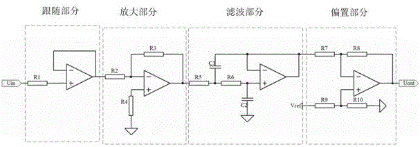
[0030] The gist of the present invention is that, through the analysis of the circuit structure and usage scenarios of the existing analog signal conditioning circuit, it is found that the existing analog signal conditioning circuit has many devices, complex circuit structure, long signal transmission distance, and occupied area. Large, high failure rate, poor economy and other problems, for the unipolar / bipolar difference of the A / D converter, it is necessary to redesign the conditioning circuit, which increases the time cost and has the problem of poor flexibility. The present invention provides a An optimized analog signal conditioning circuit and its working method to solve the above problems.

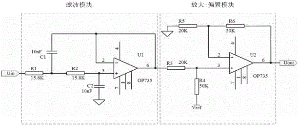
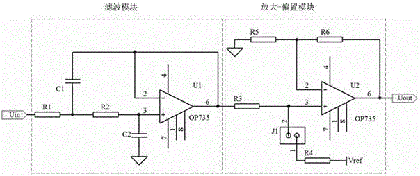
[0031] see figure 2 , the optimized analog signal con...


PUM


Abstract

The invention aims at solving the problem that according to an existing analog signal conditioning circuit, the employed devices are many, a circuit structure is complex, and the circuit design flexibility for the unipolarity/bipolarity difference of an A/D converter is relatively poor, and provides an optimized analog signal conditioning circuit and a working method thereof. The conditioning circuit comprises a filtering module composed of an active second-order low-pass filtering circuit; and an amplifier bias module composed of a bias circuit or a bias selection circuit and an amplifier circuit. An input end of the bias circuit is connected with an output end of the active second-order low-pass filtering circuit; the output end of the bias circuit is connected with the input end of the amplifier circuit; and the output end of the amplifier circuit outputs a conditioned analog signal. According to the circuit and the method, a circuit structure is optimized, the number of devices is reduced, the transmission distance is shortened, a fault rate is reduced, and the space and cost are reduced. Moreover, a working mode can be switched flexibly for the unipolarity/bipolarity of the A/D converter, the repeated design of the conditioning circuit is avoided, and the time cost is saved.

Description

technical field [0001] The present invention relates to the technical fields related to circuit design and its work, in particular to an optimized analog signal conditioning circuit and its working method. Background technique [0002] At present, the conditioning circuit is an essential part of the analog signal acquisition circuit in the power control system. The analog signal needs to be conditioned and converted into a suitable electrical quantity and sent to the sampling chip or the A / D converter that comes with the DSP. The commonly used analog signal conditioning circuit such as figure 1 As shown, it consists of 4 parts: follower module, amplification module, bias module and filter module. from figure 1 It can be seen from the figure that the existing analog signal conditioning circuit has many devices, complex circuit structure, long signal transmission distance, large occupied area, high failure rate, and poor economy. [0003] In addition, A / D converters can b...

Claims


Application Information

Patent Timeline
IPC IPC(8): H03M1/12H03H11/46
CPCH03H11/46H03M1/1245H03M1/129
Inventor 王小明罗亚桥郑国强高博谢毓广陈凡郭力徐斌计长安洪伟丁津津汪玉李远松俞斌林哲敏李圆智
Owner ELECTRIC POWER RES INST OF STATE GRID ANHUI ELECTRIC POWER
Why Eureka
Try Eureka