Test pad static releasing device and LCD
An electrostatic discharge device and test point technology, applied in the direction of instruments, nonlinear optics, optics, etc., to improve product quality and yield, reduce impact, and avoid bad products
- Summary
- Abstract
- Description
- Claims
- Application Information
AI Technical Summary
Problems solved by technology
Method used
Image
Examples
Embodiment Construction
[0019] The present invention will be further described in detail below with reference to the drawings and embodiments.
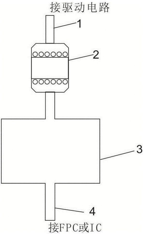
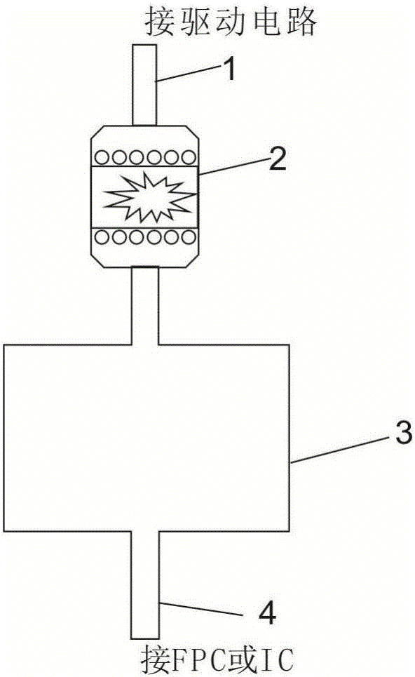
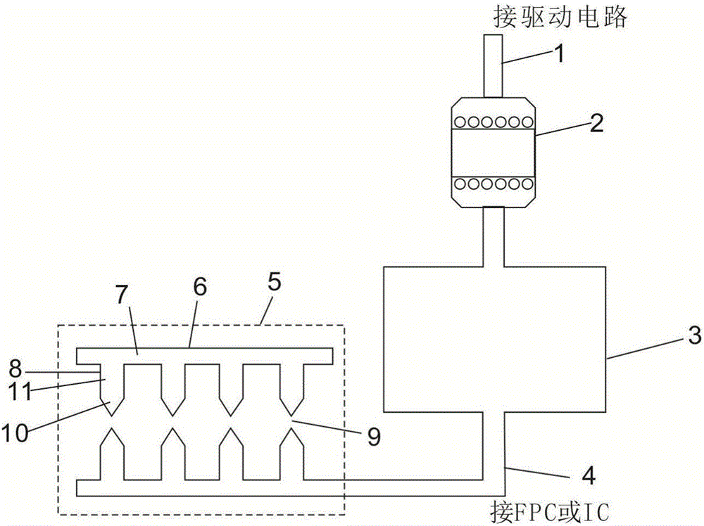
[0020] Such as figure 1 with figure 2 As shown, in the traditional LTPS process design, the structure of the non-porous test point (pad) 3 on the periphery (referring to the non-display area of the liquid crystal panel) is as follows: the non-porous test point 3 is connected in series with one end for electrostatic discharge Large resistance, electrostatic impedance (ESD) 2 is connected to the first line 1 facing the driving circuit (driving the liquid crystal panel). The specific resistance of the electrostatic impedance 2 is 50-5000 ohms, and the non-porous test point 3 passes through the second Line 4 is connected to a flexible circuit board (FPC) or an integrated circuit (IC). If the electrostatic resistor 1 is damaged by electrostatic discharge, the subsequent FPC / IC signal cannot be input, causing the product to be abnormal. The electrostatic discharge ...
PUM
| Property | Measurement | Unit |
|---|---|---|
| electrical resistance | aaaaa | aaaaa |
Abstract
Description
Claims
Application Information
 - R&D Engineer
- R&D Manager
- IP Professional
- Industry Leading Data Capabilities
- Powerful AI technology
- Patent DNA Extraction
Browse by: Latest US Patents, China's latest patents, Technical Efficacy Thesaurus, Application Domain, Technology Topic, Popular Technical Reports.
© 2024 PatSnap. All rights reserved.Legal|Privacy policy|Modern Slavery Act Transparency Statement|Sitemap|About US| Contact US: help@patsnap.com


