OLED display panel, display device, and array substrate and manufacturing method thereof

A technology of an array substrate and a manufacturing method, which is applied in the field of OLED display panels, can solve the problems of reducing the light output efficiency of OLED display panels, poor flexural resistance, and difficulty in applying flexible display devices, so as to improve utilization efficiency and improve flexural resistance. , The effect of improving the light output efficiency

Active Publication Date: 2017-02-22
SHANGHAI TIANMA MICRO ELECTRONICS CO LTD +1
View PDF3 Cites 26 Cited by
  • Summary
  • Abstract
  • Description
  • Claims
  • Application Information

AI Technical Summary

Problems solved by technology

[0004] However, the linear polarizer will also absorb 50% of the outgoing light of the display sub-pixels in the OLED display panel, which reduces the light extraction efficiency of the OLED display panel, and the linear polarizer is a multi-layer film structure, which is resistant to flex Very poor curvature, difficult to apply in flexible display devices

Method used


Image

  • OLED display panel, display device, and array substrate and manufacturing method thereof
  • OLED display panel, display device, and array substrate and manufacturing method thereof
  • OLED display panel, display device, and array substrate and manufacturing method thereof

Examples


preparation example Construction

[0094] Correspondingly, the embodiment of the present application also provides a method for preparing an array substrate, such as Figure 6 as shown, Figure 6 A schematic flow chart of the preparation method for the array substrate, including the following steps:

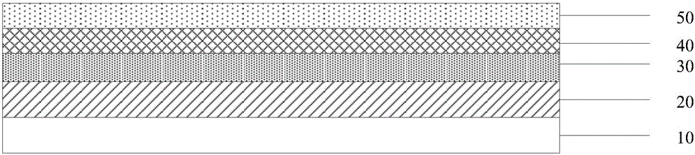
[0095] A first substrate 10 is provided.

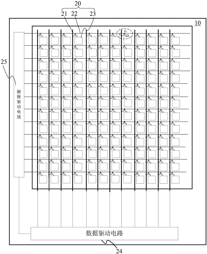
[0096] A pixel driving film layer 20 and a flat layer 30 are sequentially formed on the surface of the first substrate 10 .

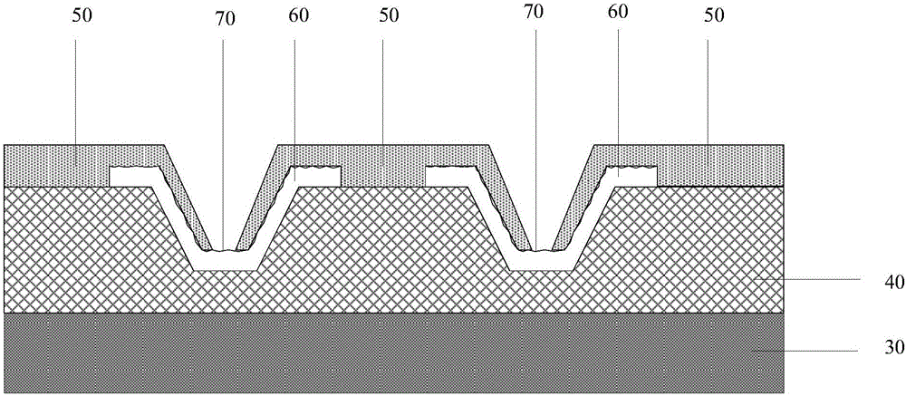
[0097] A first pixel definition layer 40 having a plurality of pixel grooves is formed on the surface of the flat layer 30 facing away from the first substrate 10 .

[0098] A reflective layer with a rough surface 70 is formed on the surface of the first pixel definition layer 40 facing away from the first substrate 10 .

[0099] An anode layer is formed on the side of the reflection layer away from the first substrate 10, and the reflection layer and the anode layer are etched, and the etched reflection layer and the anode layer completely cove...


PUM


Abstract

The application discloses an OLED display panel, a display device, and an array substrate and a manufacturing method thereof. The array substrate comprises a first substrate, a pixel drive film layer, a flat layer, a first pixel definition layer, a reflective layer, an anode layer and a second pixel definition layer. The first pixel definition layer is provided with a plurality of pixel grooves. The reflective layer is arranged on the surface of the first pixel definition layer and covers the pixel grooves completely, thereby improving the utilization efficiency of emergent light of a display sub pixel. Besides, a rough surface is formed on one side, far away from the first substrate, of the reflective layer and thus incident ambient light does not pass through the reflective layer to form mirror reflection, so that a glaring phenomenon is avoided and a problem of absorption of emergent light of a display sub pixel because of utilization of a linear polarizing film for avoidance of the glaring phenomenon can be solved. Therefore, the luminous efficiency of the display sub pixel of the OLED display panel using the array substrate is improved; and the anti-flexure performance of the OLED display panel is enhanced.

Description

technical field [0001] The present application relates to the field of display technology, and more specifically, to an OLED display panel, a display device, an array substrate and a manufacturing method thereof. Background technique [0002] With the continuous development of display technology, the application of display panels is becoming more and more extensive. Organic light emitting diode (Organic Light Emitting Diode, OLED) display panels have become the leading display panel industry due to their advantages such as fast response speed, brilliant colors, thinness and convenience. rising star. In order to improve the light extraction efficiency of the OLED display panel, it is generally necessary to arrange a reflective metal layer on the array substrate, so that the light emitted by the display sub-pixels of the OLED display panel is emitted toward one side. However, the reflective metal layer also reflects ambient light at the same time, resulting in glare and affec...

Claims


Application Information

Patent Timeline
Patent Type & Authority Applications(China)
IPC IPC(8): H01L27/12H01L21/77H01L27/32H01L51/52
CPCH01L27/1214H01L27/1259H10K59/122H10K50/856
Inventor 肖灿俊
Owner SHANGHAI TIANMA MICRO ELECTRONICS CO LTD
Why Eureka
Try Eureka