

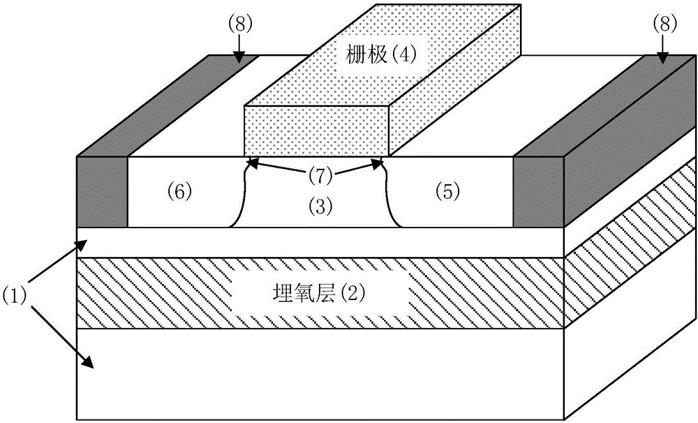
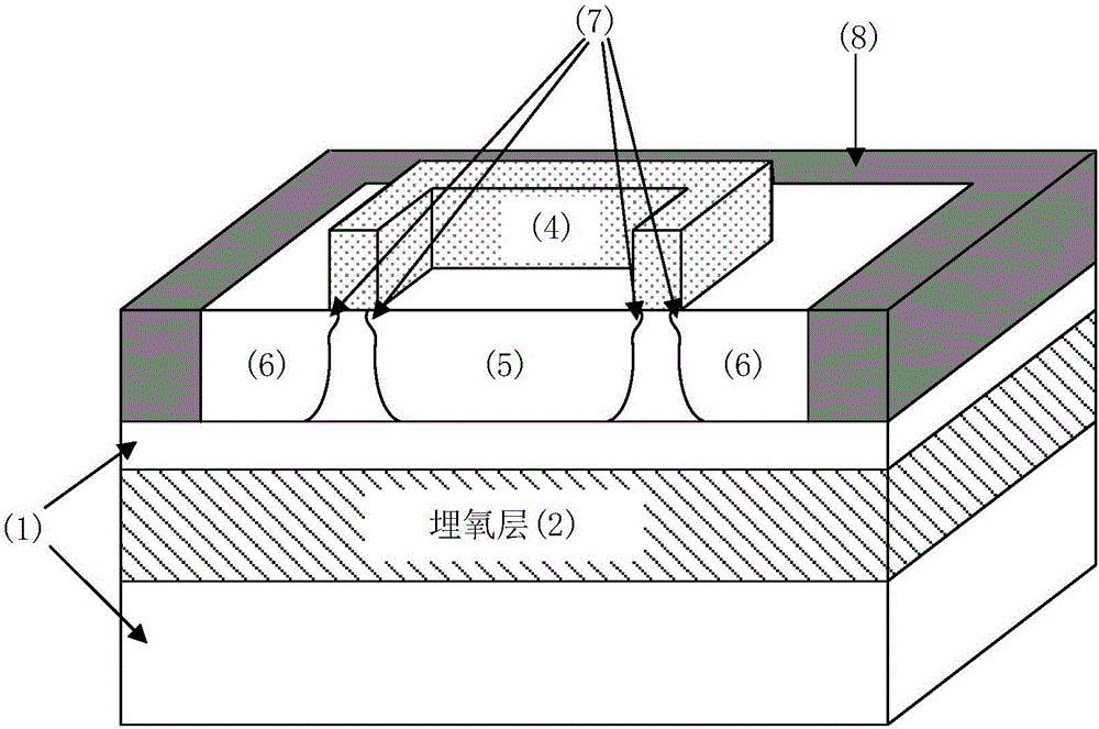
SOI (silicon on insulator) substrate based ring-gate radiation-proof MOS (metal oxide semiconductor) field-effect transistor
A field effect tube and anti-irradiation technology, which is applied in the direction of electrical components, circuits, semiconductor devices, etc., can solve the problems of device threshold voltage drift, off-state leakage current increase, sub-threshold swing degradation, etc., and achieve off-state leakage current Reduction, Leakage Current Reduction, Effect of Elimination of Effects
- Summary
- Abstract
- Description
- Claims
- Application Information
AI Technical Summary
Problems solved by technology
Method used
Image

Examples
example 1
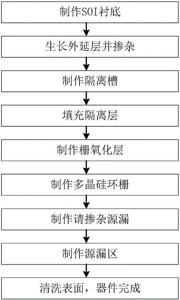
[0045] Example 1, making a SOI substrate MOS field effect transistor with a square gate ring.
[0046] Step 1, preparing an SOI substrate.
[0047] 1.1) At a temperature of 600°C, a P-type Si substrate with a thickness of 600nm was treated with a concentration of 1.7×10 18 cm -2 , Oxygen ion implantation with an energy of 180KeV;
[0048] 1.2) Annealing the P-type Si substrate after oxygen ion implantation at a high temperature of 1300°C for 5h;
[0049] 1.3) After the annealing process is completed, the prepared SOI substrate is rinsed with 5% hydrofluoric acid HF for 5 minutes, and cleaned with water for 10 minutes.
[0050] Step 2, generating an epitaxial layer.
[0051] 2.1) On the SOI substrate, grow a Si epitaxial layer with a thickness of 300nm, and the process conditions are: the reactant is SiCl 4 with H 2 ,, the temperature is 1100°C;
[0052] 2.2) The depth of the epitaxial layer is 100nm, the concentration is 2×10 17 cm -3 The boron ion doping is used to a...
example 2
[0077] Example 2, making a SOI substrate MOS field effect transistor with a rectangular gate ring.
[0078] Step 1, preparing an SOI substrate.
[0079] First, under the condition that the temperature is 650° C., the P-type Si substrate (1) with a thickness of 900 nm is treated with a concentration of 1.7×10 18 cm -2 , Oxygen ion implantation with an energy of 180KeV; then annealing at a high temperature of 1300°C for 5.5h; finally rinsing with 5% hydrofluoric acid HF for 5min, and cleaning with water for 10min.
[0080] Step 2, generating an epitaxial layer.
[0081] On the SOI substrate, through the epitaxial process at a temperature of 1100 ° C, SiCl 4 with H 2 As a reactant, grow a Si epitaxial layer with a thickness of 300nm; 17 cm -3 Doping with boron ions to adjust the channel concentration.
[0082] Step 3, etching the isolation groove.
[0083] Thin SiO with a thickness of 8 nm was grown by thermal oxidation at a temperature of 1200 °C on the epitaxial layer by ...
example 3
[0095] Example 3, fabricating a SOI substrate MOS field effect transistor with a circular gate ring.
[0096] Step A, preparing an SOI substrate.
[0097] A1) At a temperature of 700°C, a P-type Si substrate with a thickness of 1200nm was treated with a concentration of 1.7×10 18 cm -2 , Oxygen ion implantation with an energy of 180KeV;
[0098] A2) Annealing the P-type Si substrate after oxygen ion implantation at a high temperature of 1300° C. for 6 hours;
[0099] A3) After the annealing process is completed, the prepared SOI substrate is rinsed with 5% hydrofluoric acid HF for 5 minutes, and cleaned with water for 10 minutes.
[0100] Step B, substrate doping.
[0101] B1) On the SOI substrate, the SiCl 4 with H 2 As a reactant, grow a Si epitaxial layer with a thickness of 300nm;
[0102] B2) The depth of the epitaxial layer is 150nm, and the concentration is 1×10 18 cm -3 Doping with boron ions to adjust the channel concentration.
[0103] Step C, etching the i...
PUM
| Property | Measurement | Unit |
|---|---|---|
| Width | aaaaa | aaaaa |
| Width | aaaaa | aaaaa |
| Thickness | aaaaa | aaaaa |
Abstract
Description
Claims
Application Information