
Cutting technology and device for LED white-light chips

A technology of cutting process and cutting device, which is applied in the direction of electrical components, circuits, semiconductor devices, etc., can solve the problems of affecting color temperature and light spots, cutting to chips, increasing labor costs, etc., achieving simple and reliable costs, ensuring consistency, and saving costs Effect

Active Publication Date: 2017-02-22
导装光电科技(深圳)有限公司
View PDF5 Cites 5 Cited by
  • Summary
  • Abstract
  • Description
  • Claims
  • Application Information

AI Technical Summary

Problems solved by technology

The row-column spacing of chips is usually only about 0.5mm. If cutting is still carried out according to the spacing set at the beginning, the cutting track will not be on the center line between the chips, and the accumulated error after cutting may even cut to the chip. The width of the silica gel around the cut white chip is not the same, which not only affects the color temperature and light spot, but also affects the positioning during die bonding
[0004] The existing solution is through manual monitoring. When employees find that the cutting deviates from the center line, they stop and adjust, which greatly reduces efficiency and increases labor costs. Moreover, adjustments are often started only when problems arise, which cannot be fundamentally avoided.

Method used


Image

  • Cutting technology and device for LED white-light chips
  • Cutting technology and device for LED white-light chips
  • Cutting technology and device for LED white-light chips

Examples


Embodiment Construction

[0030] It should be understood that the specific embodiments described here are only used to explain the present invention, not to limit the present invention.

[0031] like Figure 5 As shown, one side of the chip 5 is in contact with the substrate, and the other five sides are covered with silica gel 6 , and fluorescent powder is uniformly mixed in the silica gel 6 . The usual array of chips 5 has a maximum size of 80mmx80mm square, the size of chips 5 usually ranges from 0.3 to 1.5mm, and the interval between rows and columns is about 0.5mm, so an array of chips 5 is about tens to hundreds of rows or columns.

[0032] The quality requirements of the white light chip 5 after cutting have two most important points: the color is consistent, and the chip 5 is in the center. The function of the phosphor is to turn the blue light of the chip 5 into white light, and the color of the white light depends entirely on the amount of the phosphor, and the color consistency means that t...


PUM


Abstract

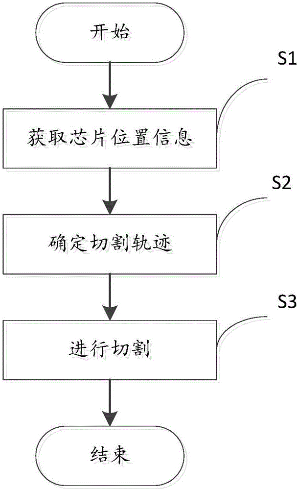
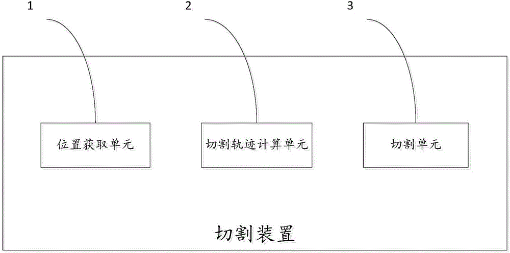
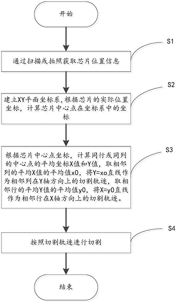
The invention discloses a cutting technology and device for LED white-light chips. The cutting technology comprises the following steps of obtaining position information of the chips, namely obtaining actual position information of the chips in a whole adhesive film; determining a cutting track, namely obtaining positions of appointed corresponding points on two adjacent rows or columns of chips according to the actual positions of the chips, calculating a mean center point of the same row or column of chips according to the positions of the appointed corresponding points in the same row or column and taking a mean value of the mean center points of two adjacent rows or columns of chips as the cutting track of the two adjacent rows or columns of chips; and carrying out cutting, namely cutting the whole adhesive film according to the obtained cutting track. The cutting technology and device have the beneficial effects that the consistency of colors and light spots is ensured; an unaccepted product or waste product of which the widths of silica gel around the chips are excessively inconsistent is avoided; the quality of the cut product is ensured; artificial monitoring and adjustment are not needed; high efficiency of automatic cutting by using a machine is brought into a full play; the cutting technology and device are simple and reliable; and the cost is reduced.

Description

technical field [0001] The invention relates to a chip cutting process, in particular to a cutting process and device for LED white light chips. Background technique [0002] CSP is the abbreviation of Chip Scale Package, and the literal translation is chip-level packaging, which refers to coating the phosphor powder on the surface and surrounding of the chip to directly make a white light chip. The production process of the white light chip is roughly as follows: First, arrange the LED blue light chips at equal intervals on the high-temperature adhesive tape. The usual array of chips ranges from several hundred to several thousand pieces, and then coat a certain thickness of phosphor powder mixed with them. Silica gel, after curing, it becomes a film with uniform thickness. One side of the LED blue light chip is in contact with the substrate, and the other five sides are covered with silica gel and phosphor; then, cut along the midline of the silica gel between the chips, s...

Claims


Application Information

Patent Timeline
IPC IPC(8): H01L33/00H01L21/78
CPCH01L21/78H01L33/0095
Inventor 董翊
Owner 导装光电科技(深圳)有限公司
Learn More