Light-emitting device and preparation method thereof

A technology for light-emitting devices and light-emitting layers, which is applied in the manufacture of semiconductor/solid-state devices, electric solid-state devices, semiconductor devices, etc., can solve the problem of inability to precisely control the distance between metal nanoparticles and light-emitting layers, and achieves the goal of improving the performance of light-emitting devices. Effect

Active Publication Date: 2017-02-22
TCL CORPORATION
View PDF6 Cites 17 Cited by
  • Summary
  • Abstract
  • Description
  • Claims
  • Application Information

AI Technical Summary

Problems solved by technology

[0006] In view of the above-mentioned deficiencies in the prior art, the object of the present invention is to provide a light-emitting device and a preparation method, aiming at solving the problem that the prior art cannot accurately control the distance between the metal nanoparticles and the light-emitting layer

Method used


Image

  • Light-emitting device and preparation method thereof
  • Light-emitting device and preparation method thereof
  • Light-emitting device and preparation method thereof

Examples


Embodiment Construction

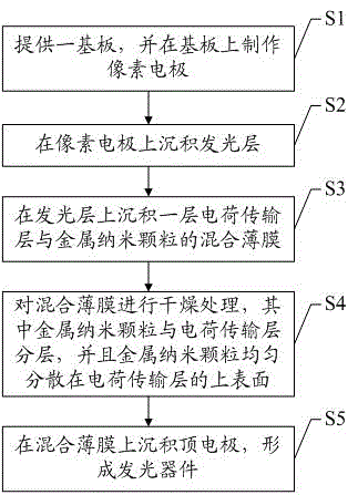
[0033] The present invention provides a light-emitting device and a preparation method. In order to make the purpose, technical solution and effect of the present invention clearer and clearer, the present invention is further described in detail below. It should be understood that the specific embodiments described herein are only used to explain the present invention, but not to limit the present invention.

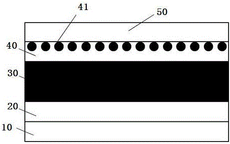
[0034] see figure 1 , figure 1 It is a schematic structural diagram of the first embodiment of a light-emitting device according to the present invention. As shown in the figure, from bottom to top, it includes: a substrate 10, a pixel electrode 20, a light-emitting layer 30, a charge transport layer 40 and a top electrode 50; Metal nanoparticles 41 are dispersed on the upper surface of the charge transport layer 40 .

[0035] In the first embodiment of the light-emitting device of the present invention, since the metal nanoparticles 41 and the charge transport layer ...


PUM

PropertyMeasurementUnit
particle diameteraaaaaaaaaa
thicknessaaaaaaaaaa

Abstract

The invention discloses a light-emitting device and a preparation method thereof. The light-emitting device comprises, from the bottom up, a substrate, a pixel electrode, a light-emitting layer, a charge transport layer and a top electrode, wherein the upper surface of the charge transport layer is distributed by metal nanoparticles. By blending the metal nanoparticles with the charge transport material, the metal nanoparticles are gathered on the surface of the charge transport layer of the light-emitting device, thereby realizing control of space between the metal nanoparticles and the light-emitting layer easily and effectively, and furthermore, improving the performance of the light-emitting device by effectively utilizing a surface plasma enhancement effect of the metal nanoparticles.

Description

technical field [0001] The present invention relates to the field of display technology, and in particular, to a light-emitting device and a preparation method. Background technique [0002] In the contemporary age of the information society, the importance of displays as a visual information transmission medium is further enhanced, and in order to dominate in the future, displays are moving towards lighter, thinner, lower power consumption, lower cost and better image quality trend development. [0003] Organic electroluminescent diodes (OLEDs) have the advantages of self-luminescence, fast response, wide viewing angle, high brightness, and thinness, and their potential market prospects are favored by the industry. Quantum dot light-emitting diodes (QLEDs) have become a strong competitor of OLEDs in recent years due to their high light color purity, high luminescence quantum efficiency, and easy tunability of luminescence colors. Therefore, these two display technologies ...

Claims


Application Information

Patent Timeline
Patent Type & Authority Applications(China)
IPC IPC(8): H01L51/50H01L51/52H01L51/56B82Y30/00
CPCB82Y30/00H10K50/14H10K50/85H10K2102/00H10K71/00
Inventor 陈亚文
Owner TCL CORPORATION
Why Eureka
Try Eureka