OLED display panel with narrow frame structure
A display panel and narrow frame technology, which is applied in the field of OLED, can solve the problems of occupying a large space and increasing the frame of OLED display, etc., and achieve the effect of increasing strength, ensuring brightness, and reducing impedance
- Summary
- Abstract
- Description
- Claims
- Application Information
AI Technical Summary
Problems solved by technology
Method used
Image
Examples
Embodiment 1
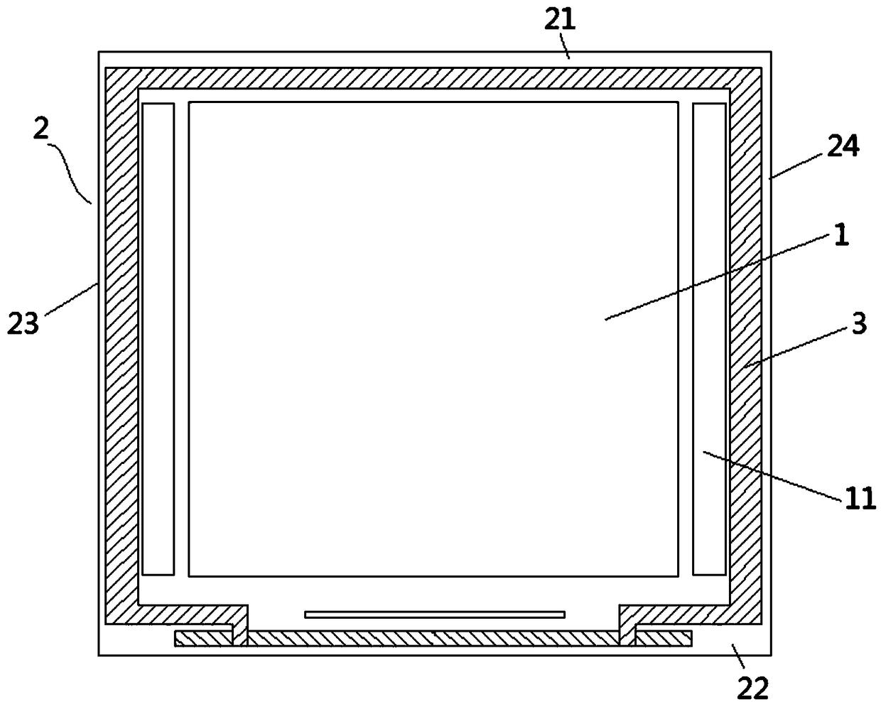
[0025] figure 2 The frame area 2 in the display area 2 includes an upper frame 21, a lower frame 22, a left frame 23, and a right frame 24. The metal wires 3 are respectively arranged in the upper frame 21 and the lower frame 22. The cathode (not shown in the figure) in the display area 1 out) is connected to the metal trace 3 through the anode. Both ends of the line 3 are electrically connected. Of course, according to different frame structures of the OLED display panel, the metal wires 3 can also be arranged on the left and right frames, and the conductive tape can be used instead of the metal wires in the upper and lower frames, so that the upper and lower frames can be made narrower.
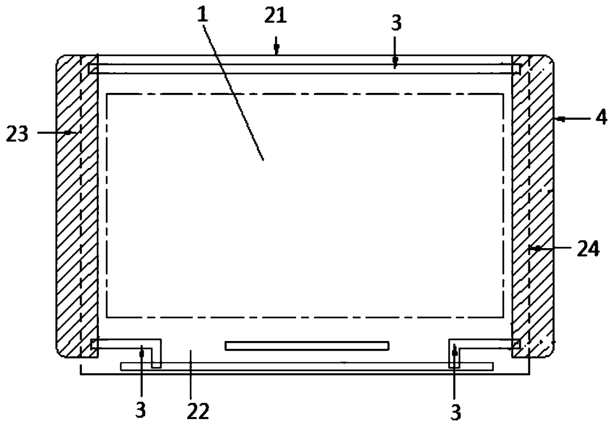
[0026] Here, the conductive tape 4 can be bonded to cover the blank area on the back of the display area 1, using a fully covered structure or a partially covered structure, thereby reducing the impedance and ensuring that the metal traces can transmit sufficient current to the OLED displ...
Embodiment 2
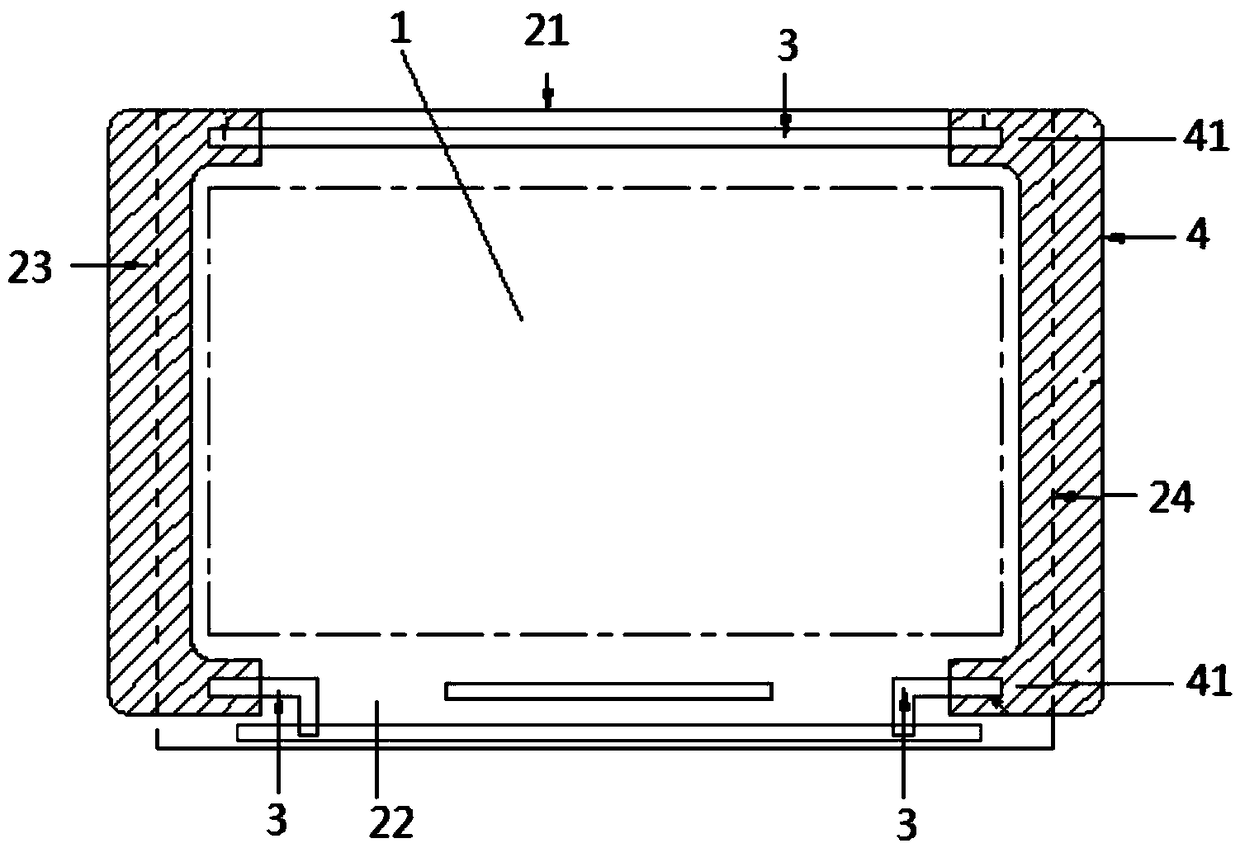
[0029] Different from Embodiment 1, in this embodiment, a raised structure 41 is formed on the upper and lower ends of the conductive tape 4 on the left frame 23 and the right frame 24 respectively, as image 3 As shown, the protruding structure 41 is located at both ends of the upper frame 21 and the lower frame 22 , and forms an electrical connection with the metal wiring 3 .
[0030] The width of the protruding structure 41 is greater than the width of the metal trace 3 . Compared with the width of the metal traces in the upper and lower frames, the conductive tape is wider to ensure that the ends of the metal traces are completely covered by the conductive tape, and because the conductive tape covers the blank area on the back of the OLED display panel, reducing the The small impedance ensures that the metal traces transmit enough current to the OLED display area, thus ensuring the brightness of the display.
[0031] Preferably, the upper end of the conductive tape 4 is f...
PUM
 Abstract
Description
Claims
Application Information


