Method for depositing insulating film on recessed portion having high aspect ratio

一种绝缘膜、凹陷部的技术,应用在电气元件、半导体/固态器件制造、电路等方向,能够解决半导体元件实现微细结构困难、绝缘特性等膜质量下降、绝缘膜困难等问题

Active Publication Date: 2017-03-08
EUGENE TECH CO LTD
View PDF4 Cites 5 Cited by
  • Summary
  • Abstract
  • Description
  • Claims
  • Application Information

AI Technical Summary

Problems solved by technology

However, it is difficult to achieve a fine structure for high integration of semiconductor elements
[0003] For example, in order to achieve a fine structure, a thinner insulating film is required, but if the thickness of the insulating film is formed thinner, there will be a problem that the film quality such as insulating properties will deteriorate
In particular, it becomes difficult to obtain a uniform and high-quality insulating film over the entire recessed portion having a high aspect ratio while forming a thin film.

Method used


Image

  • Method for depositing insulating film on recessed portion having high aspect ratio
  • Method for depositing insulating film on recessed portion having high aspect ratio
  • Method for depositing insulating film on recessed portion having high aspect ratio

Examples


Embodiment Construction

[0034] Below, refer to the attached Figure 1 to Figure 12 Preferred embodiments of the present invention are described in more detail. The embodiments of the present invention can be modified in various ways, and the scope of the present invention should not be construed as being limited to the embodiments described below. This embodiment is provided to explain the present invention in more detail to those skilled in the art to which the present invention belongs. Therefore, the shape of each element appearing in the drawings may be exaggerated in order to emphasize clearer illustration.

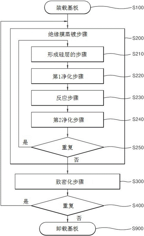
[0035] figure 1 is a flowchart showing an insulating film vapor deposition method according to an embodiment of the present invention. like figure 1 As shown, a substrate is loaded inside a cavity of a semiconductor manufacturing apparatus (S100). An insulating film is deposited on the substrate placed inside the chamber (S200). To deposit the insulating film, step S210 of forming a si...


PUM


Abstract

According to one embodiment of the present invention, a method for depositing an insulating film on a recessed portion in a substrate, in which the recessed portion having an aspect ratio of 5:1 or greater is formed, comprises: an insulating film deposition step of performing an adsorption step of injecting a silicon precursor into a chamber in which the substrate is loaded so as to adsorb silicon onto the substrate, a first purge step of removing an unreacted silicon precursor and a reaction byproduct from the inside of the chamber, a reaction step of forming the silicon, having been adsorbed, by providing a first reaction source to the interior of the chamber as an insulating film including silicon, and a second purge step of removing an unreacted first reaction source and a reaction byproduct from the interior of the chamber; and a densification step of forming a plasma atmosphere inside the chamber by applying RF power thereto, and densifying the insulating film including silicon by using the plasma atmosphere, wherein the frequency of the RF power ranges from 400 kHz to 2 MHz.

Description

technical field [0001] The present invention relates to an insulating film evaporation method, and in more detail to a method for evaporating an insulating film on a depressed portion with a high aspect ratio. Background technique [0002] Recently, with the development of the semiconductor industry and the demands of users, electronic equipment has become more and more integrated and high-performance, and semiconductor elements, which are the core components of electronic equipment, are also required to be highly integrated and high-performance. However, it is difficult to achieve a fine structure for high integration of semiconductor elements. [0003] For example, in order to realize a fine structure, a thinner insulating film is required, but if the thickness of the insulating film is formed thinner, there is a problem that the film quality such as insulating properties deteriorates. In particular, it has become difficult to obtain a uniform and high-quality insulating ...

Claims


Application Information

Patent Timeline
Patent Type & Authority Applications(China)
IPC IPC(8): H01L21/31H01L21/336
CPCH01L21/0217H01L21/02211H01L21/02219H01L21/31111H01L21/02164H01L21/02274H01L21/0228H01L21/0234H01L21/02208H01L21/473H01L21/76224
Inventor 金海元申昌勋金锡允郑春植
Owner EUGENE TECH CO LTD
Why Eureka
Try Eureka