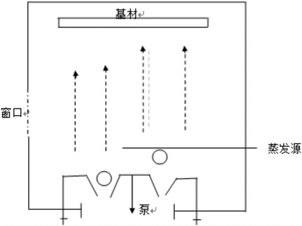
Manufacturing process of electroplating anti-reflection sapphire film onto cell phone cover plate
A manufacturing process, sapphire technology, applied to the structure of telephones, coatings, etc., to achieve convenient and fast processing, make up for low light transmittance, and improve yield
- Summary
- Abstract
- Description
- Claims
- Application Information
AI Technical Summary
Problems solved by technology
Method used
Image
Examples
Embodiment 1
[0027] 1. Chemically strengthen the surface of ordinary flat glass;
[0028] 2. Clean the strengthened glass by ultrasonic waves, and the cleaning time is 5 minutes;
[0029] 3. Vacuum electroplating process: (1) After ultrasonic cleaning, use a special umbrella to mount the film, and then perform vacuum electroplating anti-reflection film process, electroplate 6 layers of anti-reflection film, the first layer is TI3O5, the thickness is 11.41nm, the second The layer is SIO2 with a thickness of 37.54nm, the third layer is TI3O5 with a thickness of 49.52nm, the fourth layer is SIO2 with a thickness of 10nm, the fifth layer is TI3O5 with a thickness of 42.81nm, and the sixth layer is SIO2 with a thickness of 87.11 nm; (2) Vacuum evaporation and microwave thermal particle vapor deposition are used to deposit LAF3 coating material molecules on the surface of the substrate to form a sapphire film with a thickness of 40nm; (3) Vacuum electroplating oil-resistant film technology is us...
Embodiment 2
[0032] 1. Chemically strengthen the surface of ordinary flat glass;
[0033] 2. Clean the strengthened glass by ultrasonic waves, and the cleaning time is 10 minutes;
[0034] 3. Vacuum electroplating process: (1) After ultrasonic cleaning, use a special umbrella to mount the film, and then perform vacuum electroplating anti-reflection film process, electroplate 6 layers of anti-reflection film, the first layer is TI3O5, the thickness is 23.54nm, the second The layer is SIO2, the thickness is 27.69nm, the third layer is TI3O5, the thickness is 61.31nm, the fourth layer is SIO2, the thickness is 29.34nm, the fifth layer is TI3O5, the thickness is 38.46nm, the sixth layer is SIO2, the thickness is 69.76nm; (2) Vacuum evaporation and microwave thermal particle vapor deposition are used to deposit LAF3 coating material molecules on the surface of the substrate to form a sapphire film with a thickness of 35nm; (3) Vacuum electroplating oil-resistant film technology is used, and the...
PUM
| Property | Measurement | Unit |
|---|---|---|
| Thickness | aaaaa | aaaaa |
| Thickness | aaaaa | aaaaa |
| Thickness | aaaaa | aaaaa |
Abstract
Description
Claims
Application Information

