Check patentability & draft patents in minutes with Patsnap Eureka AI!

Thin film transistor array substrate and manufacturing method thereof

A technology of thin film transistors and array substrates, applied in the field of thin film transistor array substrates and its production, can solve the problems of low off-state current, etc., and achieve the effects of improving off-state current, good potential holding capacity, and simple manufacturing process

Active Publication Date: 2017-03-15
WUHAN CHINA STAR OPTOELECTRONICS TECH CO LTD
View PDF5 Cites 8 Cited by
  • Summary
  • Abstract
  • Description
  • Claims
  • Application Information

AI Technical Summary

Problems solved by technology

[0012] For the display panel, the TFT in the driving circuit area is used for logic circuits and needs to have a large on-state current; however, the TFT in the display area needs to have a good potential holding capacity and a low off-state current, that is to say , the thin film transistor array substrate prepared according to the prior art cannot meet this requirement

Method used


Image

  • Thin film transistor array substrate and manufacturing method thereof
  • Thin film transistor array substrate and manufacturing method thereof
  • Thin film transistor array substrate and manufacturing method thereof

Examples


Embodiment Construction

[0049] In order to further illustrate the technical means adopted by the present invention and its effects, the following describes in detail in conjunction with preferred embodiments of the present invention and accompanying drawings.

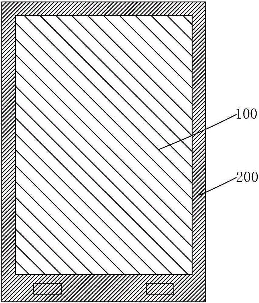
[0050] see Figure 4 , the present invention firstly provides a thin film transistor array substrate, including a display area 10 and a drive circuit area 20 arranged on the periphery of the display area 10, a display area TFT is arranged in the display area 10, and a display area TFT is arranged in the drive circuit area 20 There is a TFT in the driving circuit area;

[0051] Wherein, the material of the active layer of the TFT in the display area and the active layer of the TFT in the driving circuit area is low-temperature polysilicon; the current conduction direction of the channel of the TFT in the display area is perpendicular to that of the TFT in the driving circuit area. The direction of current conduction in the channel.

[0052] I...


PUM


Abstract

The invention provides a thin film transistor array substrate and manufacturing method thereof. According to the thin film transistor array substrate, a current conduction direction of a channel of a display area TFT is vertical to an ELA laser scanning direction, so that crystal grain arrangement of the channel of the display area TFT in the current conduction direction is relatively unordered, and off-state current of the display area TFT is reduced, so that the display area has a relatively good potential maintaining capability; at the same time, a current conduction direction of a channel of a driving circuit area TFT is parallel to an ELA laser scanning direction, so that crystal grain arrangement of the channel of the driving circuit area TFT is relatively ordered in the current conduction direction, and off-state current of the driving circuit area TFT is improved, thereby improving the field mobility and output current characteristic of the driving circuit area; and the thin film transistor array substrate provided by the invention can satisfy different characteristic requirements of the display area TFT and driving circuit area TFT, thereby improving an overall display effect of a display panel.

Description

technical field [0001] The invention relates to the field of display technology, in particular to a thin film transistor array substrate and a manufacturing method thereof. Background technique [0002] Thin Film Transistor (TFT for short) is currently the main component in Liquid Crystal Display (LCD for short) and Active Matrix / Organic Light-Emitting Diode (AMOLED for short) The driving element is directly related to the development direction of the high-performance flat panel display device. There are many kinds of materials for preparing the active layer of thin film transistors. Low Temperature Polysilicon (LTPS) material is one of the more preferred materials. Due to the regular arrangement of atoms of low temperature polysilicon, the carrier mobility is high, and the voltage For driven liquid crystal display devices, low-temperature polysilicon thin-film transistors can use smaller thin-film transistors to realize the deflection driving of liquid crystal molecules du...

Claims


Application Information

Patent Timeline
IPC IPC(8): H01L27/12H01L21/84
CPCH01L27/1222H01L27/1285
Inventor 王涛
Owner WUHAN CHINA STAR OPTOELECTRONICS TECH CO LTD
Features
  • R&D
  • Intellectual Property
  • Life Sciences
  • Materials
  • Tech Scout
  • Unparalleled Data Quality
  • Higher Quality Content
  • 60% Fewer Hallucinations
Learn More