

An organic thin film transistor with improved subthreshold swing and switching ratio and its preparation method
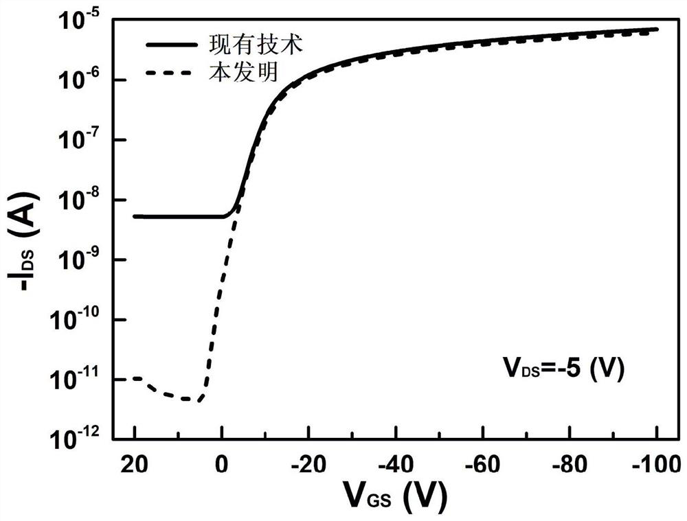
A sub-threshold swing, organic thin-film technology, applied in semiconductor/solid-state device manufacturing, semiconductor devices, electric solid-state devices, etc. On/off ratio, good electrical performance, effect of reducing on-state current
- Summary
- Abstract
- Description
- Claims
- Application Information
AI Technical Summary
Problems solved by technology
Method used
Image

Examples
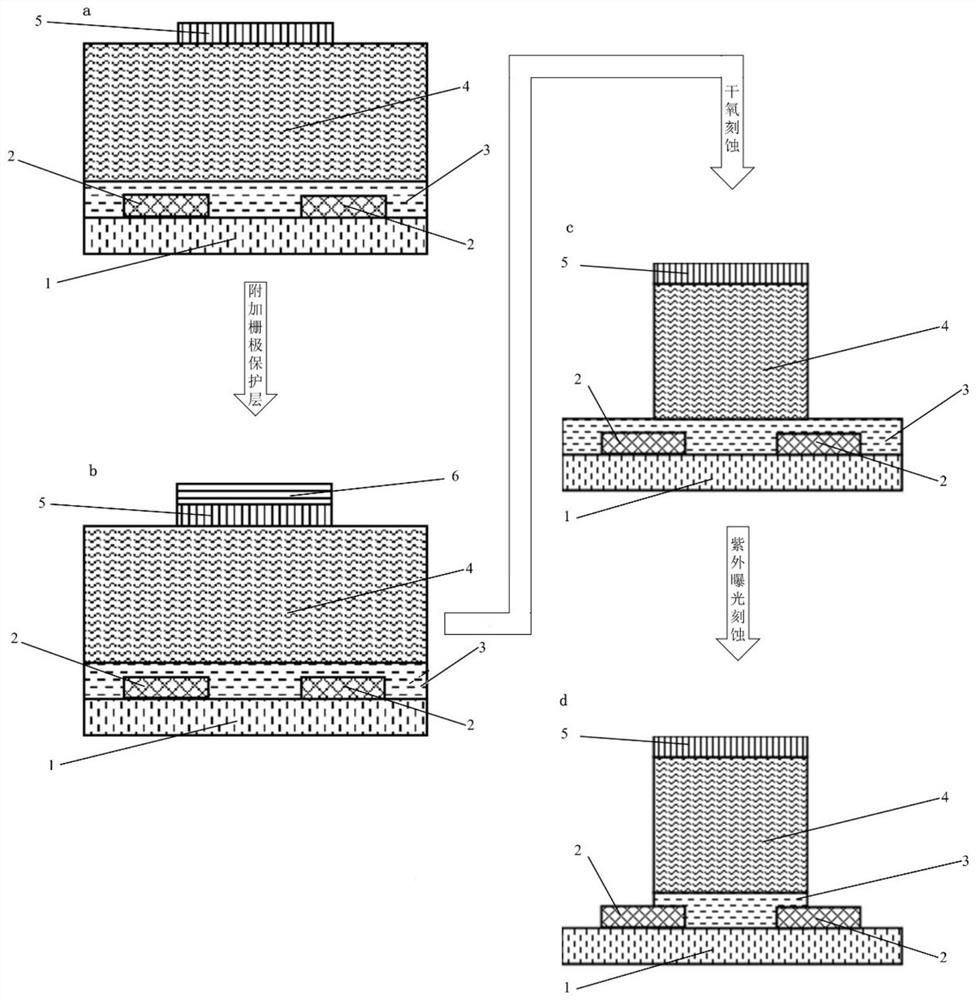
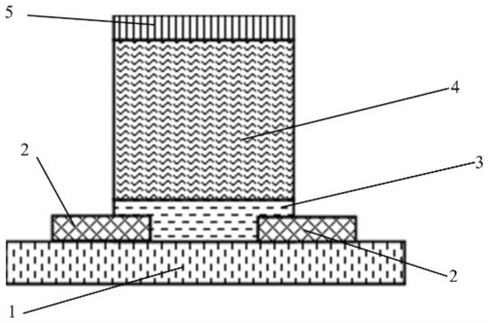
Embodiment 1
[0053] Step 1: 1,4-dioxodipyrrole and thiophene polymer (DPPT-TT) was dissolved in dichlorobenzene at a ratio of 8 mg / ml, and stood on a heating plate at 70°C for 24 hours.
[0054] Step 2: Dissolve polymethyl methacrylate in butyl acetate at a ratio of 50 mg / ml and let stand on a heating plate at 70°C for 24 hours.
[0055] Step 3: Select a 1.5 cm x 1.5 cm glass slide as the substrate, ultrasonically clean it in deionized water, acetone, and isopropanol for 15 minutes, and finally dry it with a nitrogen gun.
[0056] Step 4: Using a vacuum thermal evaporation method, using a stainless steel mask, vapor-deposit gold electrodes with a length of 100 microns, a width of 1000 microns, and a thickness of 50 nanometers on the substrate as source and drain electrodes.
[0057] Step 5: Put the solution prepared in step 1, through a pipette gun, onto the glass slide treated in step 4, spin coating at 4500 rpm for 40 seconds, and place on the source and drain electrodes A semiconductor...
PUM
| Property | Measurement | Unit |
|---|---|---|
| thickness | aaaaa | aaaaa |
Abstract
Description
Claims
Application Information